The ability of Nikon Corporation to supply both globally renowned digital cameras, alongside high-end optics made from glass manufactured in its own factory in Japan, has secured a repeat microscopy sale at the Hahn-Schickard Institute for Micro and Information Technology in Villingen-Schwenningen, south-west Germany. Hahn-Schickard also operates from locations in Freiburg, Ulm and Stuttgart, specializing in harnessing microsystem technologies across all industries to develop intelligent products from conception through to small, medium or large-scale manufacture. Their innovative products and technologies are found in the areas of micro-electromechanical systems (MEMS), lab-on-a-chip, sensors and actuators, cyber-physical systems, information technology, software development and analytics. 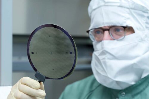 The non-profit research and development service provider for microsystem technology requires a large array of 2D and 3D inspection strategies, measurement and test equipment including white light interferometry, X-ray CT and benchtop scanning electron microscopy capabilities to support its research and pre-production activities. Extensive use is also made of light microscopes, three Nikon binocular compound microscope models having underpinned much of this work for many years. David Hochstein, Process Engineer and Research Associate in Villingen-Schwenningen, who has special responsibility for photolithography in semiconductor chip production from wafers up to 150 mm said, “Our existing Nikon microscopes were fitted with older camera technology that was not compatible with the current Windows 10 operating system, so we decided to purchase new cameras as part of a planned modernization program. “It was also clear that to be able to meet the increasing throughput of measuring and testing that has to be carried out, we would need an additional microscope to expand capacity.
Although we evaluated other potential sources of microscopes, Nikon was our preferred choice of supplier as a lot of engineers here are familiar with and happy to use the software, so only a short training period was needed.
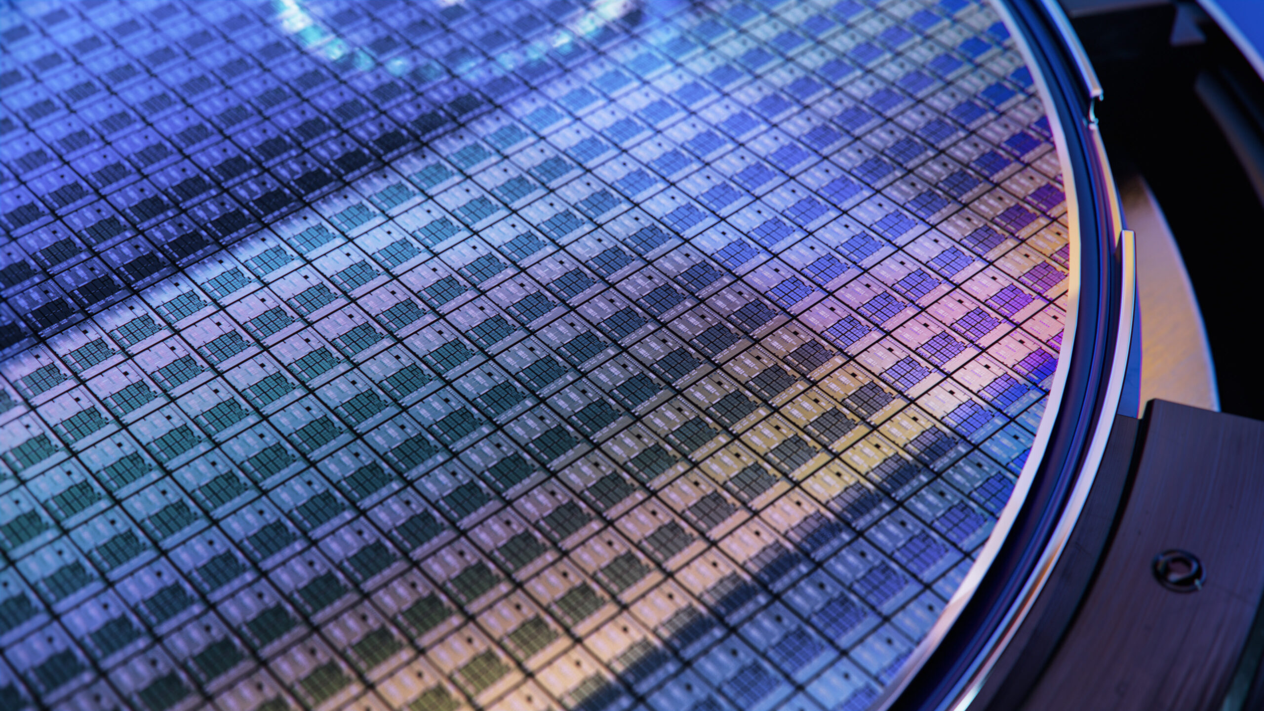
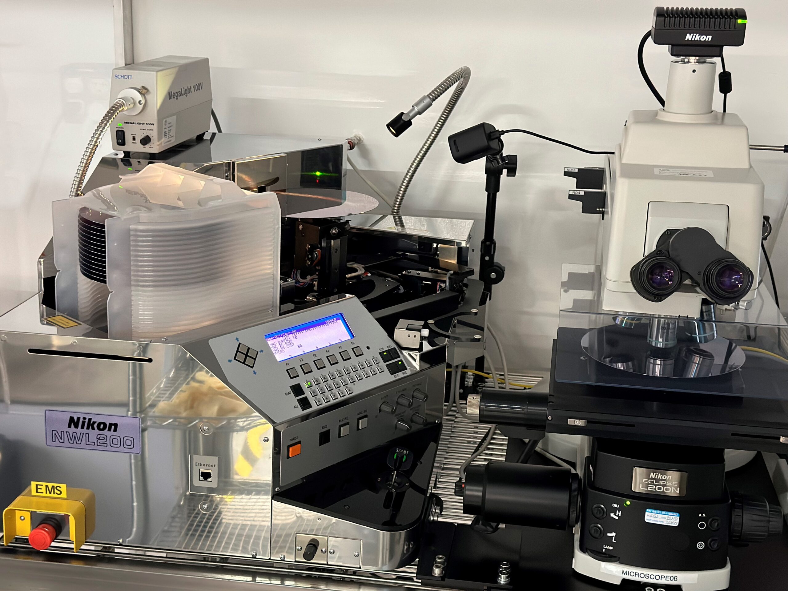
Consequently, Hahn-Schickard bought an Eclipse L200ND large stage ‘semiconductor’ microscope from Nikon Metrology with a Digital Sight DS-Fi3 digital camera, plus an additional three of the latter so that the existing optical microscopes could be similarly equipped. The cameras have a 5.9 megapixel CMOS image sensor and high-speed data readout, superior color reproduction, and high quantum efficiency for optimal imaging in various observation modes including brightfield, darkfield, differential interference contrast (DIC), phase contrast and fluorescence excitation. The latest trinocular compound microscope with camera port includes Nikon Metrology’s CFI60-2 optics that have been shown to be a perfect fit for the inspection of integrated circuits, flat panel displays, large scale integration electronic devices and the latest types of wafer using both episcopic and diascopic optical contrast methods. Combining these superior optics with the many different types of illumination delivers exceptional high contrast and resolution, with darkfield contrast images are now three times brighter than was previously achievable. Up to six objectives can be mounted at the same time. Excellent parfocality and parcentricity of lenses minimizes shifting of the image when the objective is changed, saving time by avoiding disorientation on the region of interest. It allows stable observation from high to low magnification while maintaining image position. The SEMI S2-0200/S8-0600-compliant eyepiece, positioned close to the operator for ergonomic operation, has an ultra-wide 25mm field of view and observation tube angle adjustment between 0 and 30 degrees. Completing Hahn-Schickard’s latest purchase was a Nikon Metrology’s NIS-Elements imaging and archiving software suite, which manages the DS cameras to capture optimal images quickly, organize them and carry out visualization and analysis in a smooth workflow. Powerful features are included such as image stitching, object counting and volume views. The particular version supplied to the research and development service provider was NIS-Elements BR (basic research) for use with fluorescent excitation imaging and is capable of data management and analysis of up to four dimensions – for example X, Y, Z and Lambda (wavelength). Mr. Hochstein concluded, “The higher resolution images that the latest equipment produces extends from the visible spectrum into the infrared, which is especially useful for photolithography. Moreover, switching between infrared and visual inspection is fast. “We are very familiar with Nikon equipment, so we were able to install the systems ourselves and avoid any coronavirus issues. We have always received excellent support from this supplier and in particular from their Dr. Peter Callsen-Cencic, who is based at Nikon Metrology GmbH in Alzenau.”


