The introduction of a programmable video measuring system with automatic handling of semiconductor wafers by the Industrial Metrology Business Unit of Nikon Corporation has halved the capital cost of setting up an AOI (automated optical inspection) facility for wafer-level quality control during IC (integrated circuit) manufacture. As scanning sequences can be tailored to suit a customer’s requirements, downtime prior to conversion is reduced compared with using conventional AOI systems, allowing better control of wafer-level processes by having a tool that meets different requirements.
The problem with expensive, dedicated AOI hardware on the market is that it is designed to follow a strict procedure of autonomous, zig-zag scanning of an entire post-lithography wafer surface to collect data on any defects that may be present. In contrast the flexible, low-cost Nikon solution is essentially an optical coordinate measuring system that can be programmed to execute a shorter, more pragmatic inspection cycle to suit each quality control requirement.
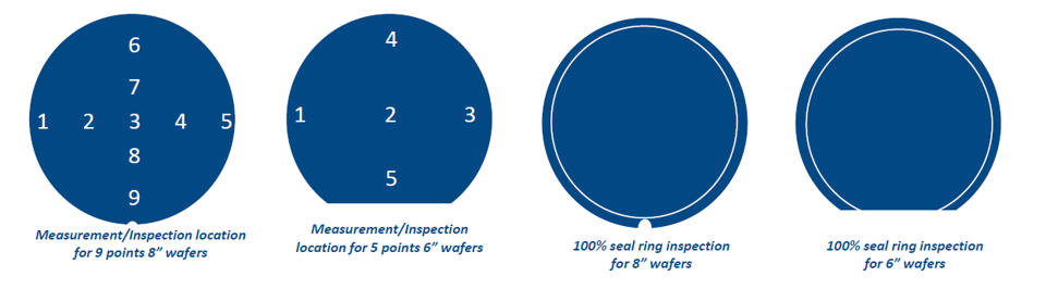
The new quality optimization procedure is best described by looking at a pilot installation recently completed in Singapore. The customer did not want to carry out critical dimension checks on dies over the whole area of an 8-inch (200 mm) diameter wafer, as it was not necessary for obtaining reliable results. Instead, scanning was needed around the full circumference plus a few regularly-spaced, isolated locations nearer to the center. Similar was required for 6-inch (150 mm) diameter wafers.
High throughput of the system is ensured by a Nikon NWL200 automatic wafer loader, which transfers each wafer from a cassette to the video measuring machine and returns it after inspection, without any need for human intervention. Any faulty wafers are reworked, while good wafers are sent downstream for back-end operations. For system monitoring and tracking, the graphical user interface employs the industry-standard SECS/GEM protocol for equipment-to-host data communication.
The compact automation system is characterized by having a high mean time before failure and low maintenance costs. Once the wafer has been loaded onto the NEXIV VMZ-S3020, image capture and measurement in nine central areas of an 8-inch wafer takes about 10 seconds and wafer edge inspection is completed in a four-minute cycle that produces 180 images for analysis.
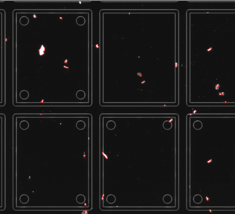
Selection of the specific areas and programming of the Nikon NEXIV VMZ-S3020 video measuring machine to inspect them is straightforward using standard software, AutoMeasure. Another feature of the video measuring machine is its use of a variety of illumination options, including both brightfield and darkfield, which are programmed to turn on and off during an inspection cycle. The former highlights photoresist staining well, while the latter is better for resolving the presence of scratches on the silicon surface. Both are able to identify the existence of particulates that might cause shorting or otherwise adversely affect eventual IC function.
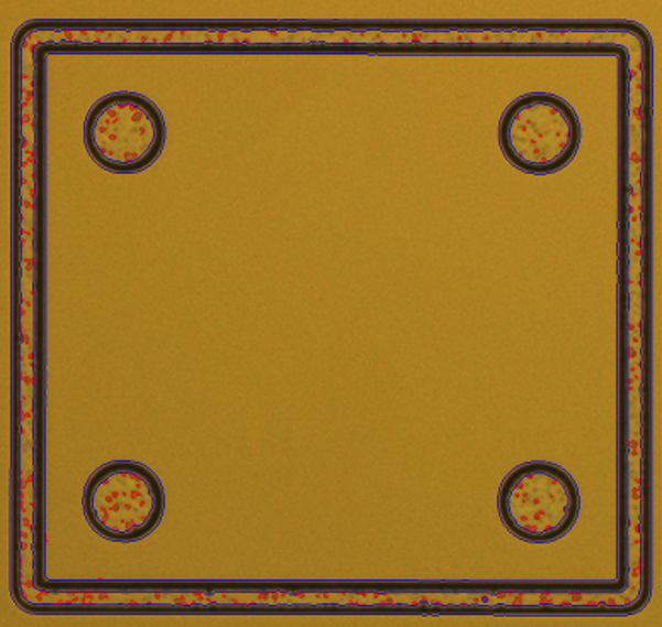
For example, using darkfield illumination it is possible to detect particles that have higher gray-level intensity compared to the background and wafer patterns. With brightfield, defects may be detected by checking the difference in contrast. Wafer edge inspection enables defects to be seen inside the seal ring by looking at the intensity level.
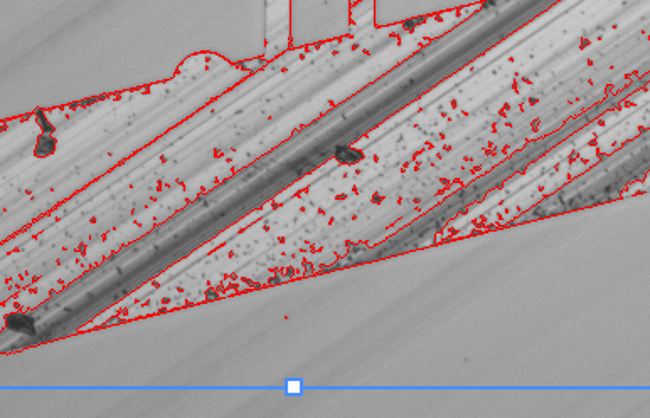
Another notable feature of the NEXIV VMZ-S is the use of proprietary linear encoders with 0.01 μm resolution in all axes, so track widths down to 0.8 μm for high accuracy Critical Dimension, CD metrology. Further details are available here.


