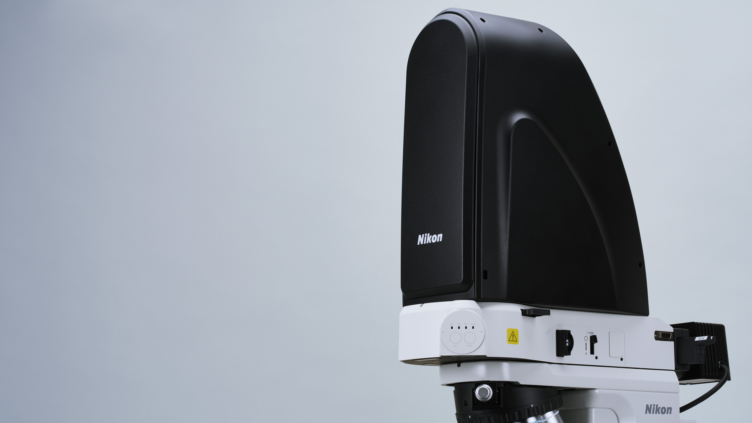
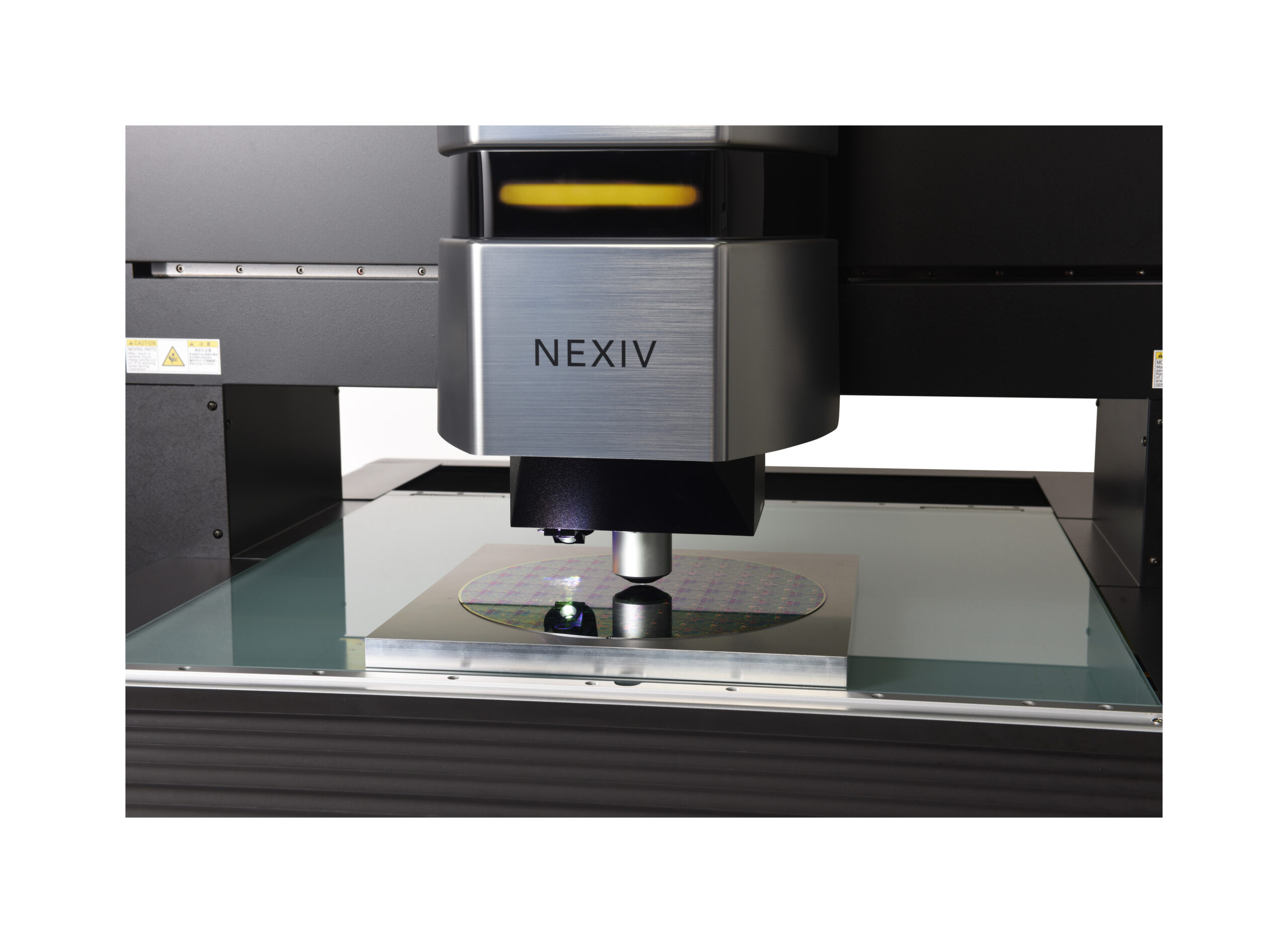
The Industrial Metrology Business Unit of Nikon Corporation has released the automatic wafer measurement system NEXIV VMZ-NWL 200 to solve the challenges of wafer metrology in the semiconductor back-end process, where more work is traditionally carried out manually than in front-end process control. The main target market for NEXIV VMZ-NWL 200 is therefore measurement centered on semiconductor manufacturing processes in the back-end.
NEXIV VMZ-NWL 200 alleviates the shortage of skilled technicians for manual measurement. The semiconductor industry has developed along the path of miniaturization, which has increased the skill level required for measurement and reduced the number of available engineers. On the other hand, the semiconductor market continues to expand so the increasing metrology opportunities are being offered to ever fewer people. As a result, manual measurements using conventional optical microscopes have reached their limits.
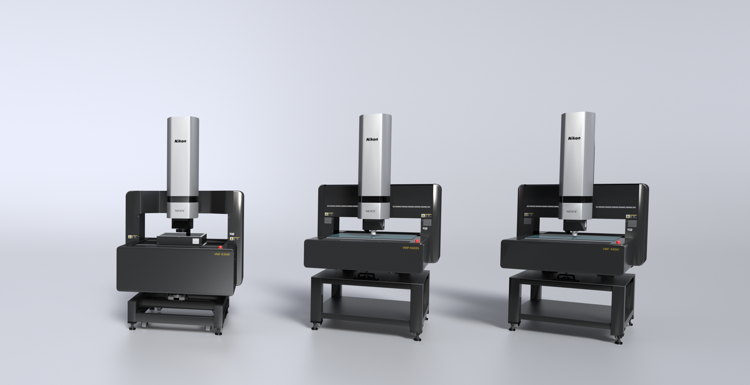
NEXIV VMZ-NWL 200 is a system that automatically measures 6-inch or 8-inch wafers held in a carrier according to a measurement program. High repeatability of measurement is ensured by the reliability of the NEXIV and stable wafer loading using the NWL. The system allows intuitive selection of the chip to be measured using dedicated software. Therefore, anyone is able to achieve the chip measurement results they need with a high degree of reliability. In addition, it is possible to trace when the measurement was performed and by which program, helping to improve traceability.
The system is designed with safety in mind and a protective cover is provided to prevent possible damage due to operator error. Operation meets SEMI international standards S2, S8, and F47.
-600x338.png)
About Nikon Metrology
Nikon provides a variety of products, services, and solutions worldwide, based on advanced optoelectronics and precision technologies cultivated during the company’s more than 100 years of history. The group continues to create new values that contribute to improvement of quality of life and manufacturing in a wide variety of forms. Nikon’s Industrial Metrology Business Unit (IMBU) delivers integrated, optimized, ultra-high precision solutions that are not only customized and cost-effective but also work extremely well as soon as they are implemented. A recent development under Nikon’s Digital Manufacturing banner is closer cooperation between IMBU and the corporation’s Digital Solutions Business Unit (DSBU), which has launched a series of optical additive and subtractive manufacturing solutions for processing a wide variety of materials for the sub-micron surface finish. www.industry.nikon.com
Media Contact:
Nikon Metrology, LLC – Americas
12701 Grand River Road
Brighton, MI 48116 USA
Contact: Amanda Bourque, Lead Generation & Marketing Assistant
Email: [email protected]
Web: www.industry.nikon.com/en-us/