
The semiconductor industry represents the extreme edge of innovation and operational efficiency. Critical test and inspection applications include analysis to detect defective chips, optimize yield, and verify electrical/physical parameters.
Nikon will address these requirements with three product lines on display at SEMICON West:
- Microscopy. Nikon industrial and measuring microscopes offer exceptional resolution of surfaces through wide magnification ranges, ideal for measuring 2D and 3D features and failure analysis.
- Video Measuring. Nikon’s vision systems offer a range of high-quality optics, high-speed scanning, and nonstop automated measurement, providing perfect solutions for capturing tiny features and challenging edges.
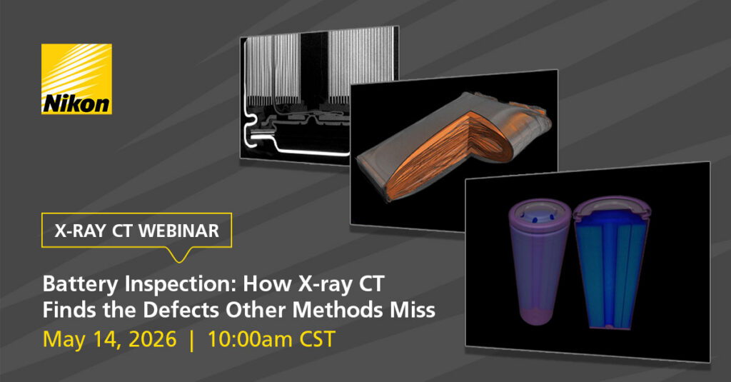
- X-ray CT. We offer a line of X-ray and CT systems and quick-turn inspection services providing non-destructive inspection solutions for R&D and quality control applications.
