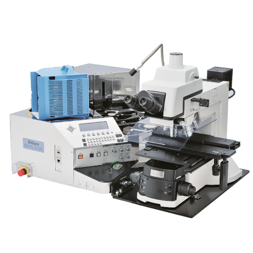
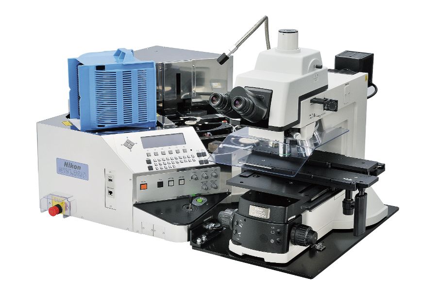
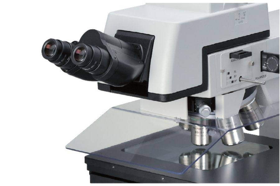
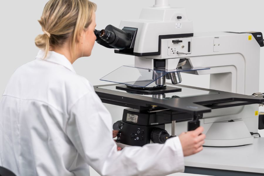
Products and promotions may differ based on your selected region.
Superb Nikon CFI60-2 optics provide excellent images to both eyepieces and also to Nikon’s digital imaging cameras with analysis software. Combining these superior optics with an extraordinary illumination system delivers images of excellent contrast and resolution.
These microscopes are for exceptionally precise optical inspection of wafers (200mm for L200N series and 300mm for L300N series), reticles and other substrates.
Nikon’s innovative design enables clear imaging techniques, including high contrast, brightfield, darkfield, polarization (POL), differential interference contrast (DIC) and double beam interferometry optical contrast.
The full range of Nikon’s Digital Sight cameras efficiently captures images of a sample and deliver them to the image processing software of the NIS-Elements suite, together with microscope data on the objective lens used, magnification setting and light intensity.
Nikon wafer loaders are well accepted and trusted in the semiconductor industry and many installations are in use today.
Nikon’s innovative design enables clear imaging techniques, including high-contrast, brightfield, darkfield, polarization (POL), differential interference contrast (DIC) and double beam interferometry optical contrast.
Reflected light: brightfield, darkfield, polarizing (POL), differential interference contrast (DIC), epi-fluorescence and two-beam interferometry. Transmitted light: brightfield, darkfield, polarizing, differential interference contrast and phase contrast.
The microscope detects and controls the objective lens in use, light intensity, episcopic illumination and aperture via a USB connection to Nikon’s NIS-Elements software.
Optimal positioning of operator controls and a variable angle eye-tube allows fatigue-free work. A right-way-up, right-way-around image is provided for correctly observing raw materials, semiconductors and industrial components.
Applications are centered around inspection duties in the electronics and telecommunications sectors. Antenna waveguides are measured with utmost precision, as well as other components such as wafers for semiconductor or photovoltaic devices and micro electro mechanical systems (MEMS) used in smartphones, gyroscopes and accelerometers, for example.
If you would like further details on this product or a more in-depth description, our expert team will provide you with additional information and, if required, arrange an on-site visit. Talk to us in detail about your project and our experts will advise you on the best inspection system to meet your requirements. Please fill out the form opposite and we will get in touch with you shortly.