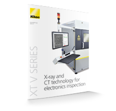
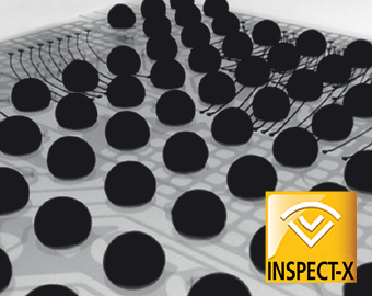
Inspect-X for XT V Series
Designed around the user experience, Inspect-X software provides intuitive displays, advanced imaging and a suite of analysis tools for the XT V, XT H and LES system ranges.
Discover the Product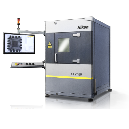
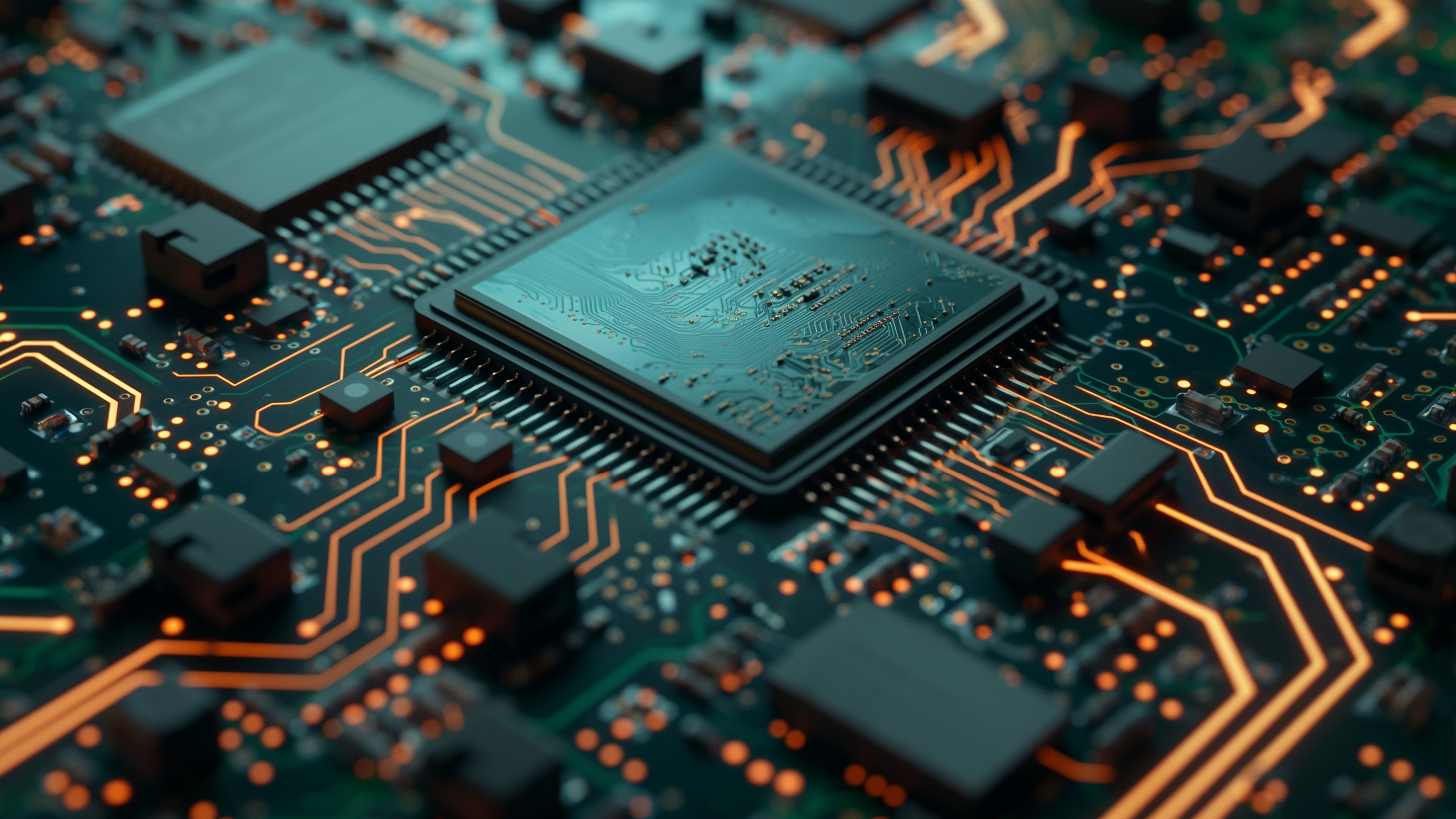
The XT V series enables insights into printed circuit board assemblies, components, or electrical devices in an intuitive, non-destructive inspection process. X-ray inspection provides many benefits to manufacturers and researchers alike, accelerating throughput and improving product quality – all whilst reducing costs.


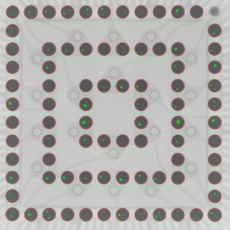
Set up an automated inspection program in minutes with the intuitive Inspect-X interface – no programming required! PCB Analysis Suite is capable of advanced measurement and analysis of BGA, bond wires, PTH and complex packages such as PoP on multi-layered boards, with automated pass/fail inspection and reporting.
Automatic collision avoidance prevents physical damage to the system and sample, even at maximum magnification. Low Dose Collimator minimises X-ray exposure, enabling detailed batch inspection of semiconductor devices. ESD Safety Upgrade keeps samples safe from harm, compliant with global standards.
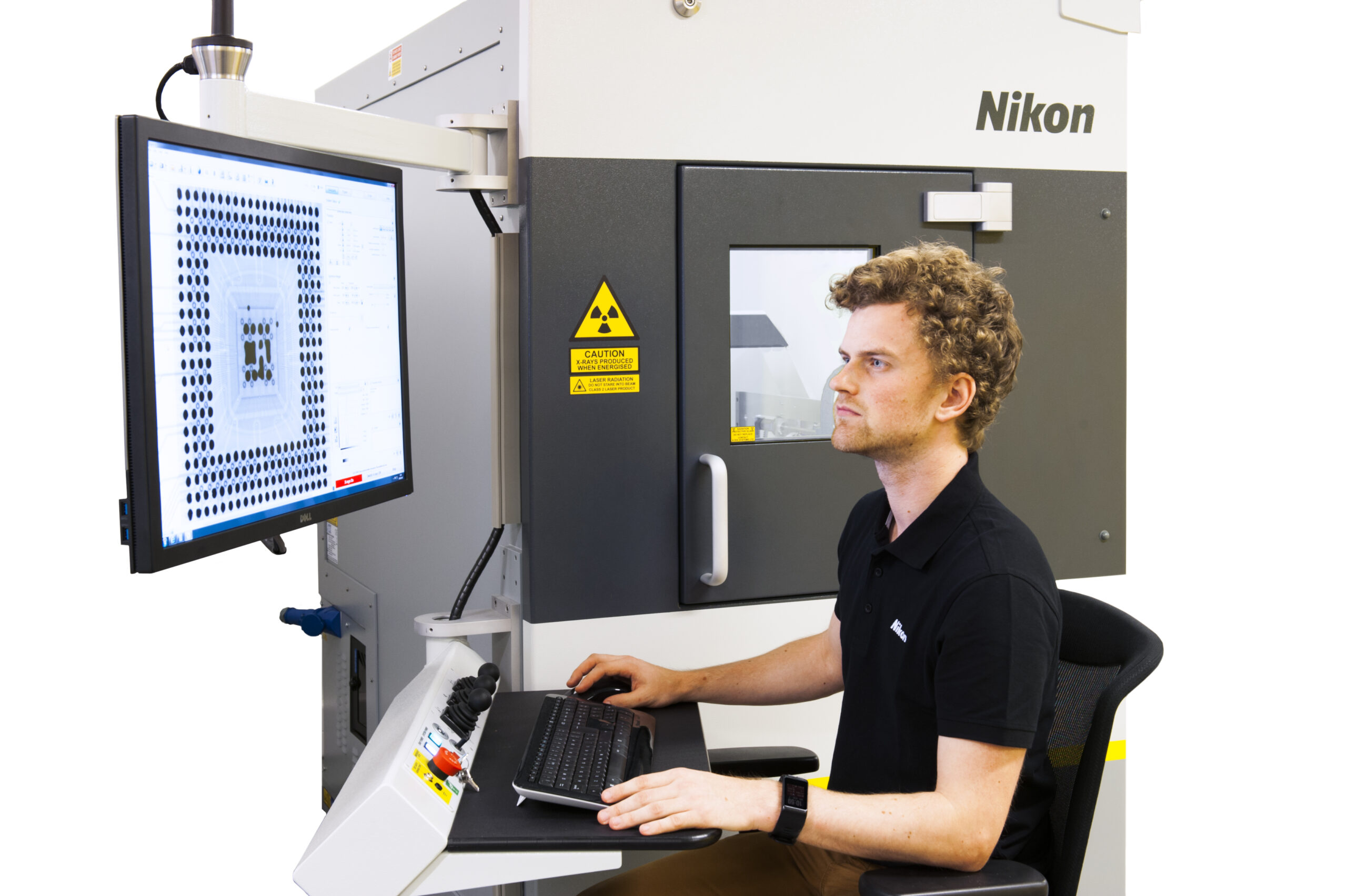
The vertical system configuration, with the X-ray source below the sample tray and the tilting imager above, is controlled through user-friendly Inspect-X software or via precise joystick manipulation. Even at an extreme oblique angle view, intelligent motion control keeps the region of interest in view throughout 360° sample rotation.
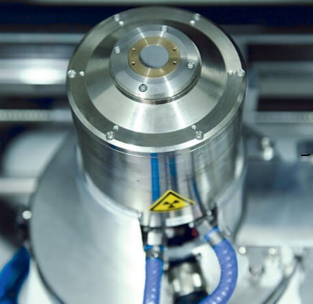
Nikon’s market-leading Xi microfocus X-ray sources provide a sharp, stable and bright image. The Diamond Window improves contrast across the full operating range, making fine defects easier to spot. In-house open tube design with integral generator reduces cost of ownership and improves reliability, with minimal maintenance required.


High Contrast Filter 2.0 reveals hidden details in radiography images by providing outstanding image quality of both high and low contrast areas in a single clear image with no colour adjustment. Operators can now identify all aspects of the sample more quickly than ever before, optimising and increasing their productivity.

| XT V 160 | XT V 130C | |
| Maximum kV | 160 kV | 130 kV |
| X-ray source | Open tube with replaceable filaments for unlimited lifetime | |
| High voltage generator | Integrated generator - no HV cable maintenance required | |
| Feature recognition | Submicron | Micron-level |
| Viewing angle range | Up to 82° in any direction | Up to 79° in any direction |
| Sample tray | Carbon fibre tray, 580 mm (22.8 ") diameter | |
| Cabinet dimensions (W x D x H) | 1,260 x 1,789 x 1,904 mm (50 x 70 x 75 ") | |
| System weight | 2,100 kg (4,630 lbs) | |
| ESD safety | ESD-safe to industry standards with optional ESD Safety Upgrade | |
| Primary applications | Automated and real-time electronics and semiconductor inspection for R&D, QA, QC and failure analysis | Real-time electronics inspection |
Electronics manufacturing demands precision inspection of complex assemblies. The XT V Series provide the resolution and flexibility to detect defects in BGAs and analyse bond wire integrity. The ESD Safety Upgrade and Low Dose Collimator ensure sensitive components remain protected throughout the inspection process. The PCB Analysis Suite is capable of advanced measurement and analysis of BGA, bond wires, PTH and complex packages such as PoP on multi-layered boards, with automated pass/fail inspection and reporting.

Semiconductor devices require careful handling and precise inspection. The Low Dose Collimator minimises radiation exposure to sensitive devices, while the ESD Safety Upgrade enables ESD-safe inspection, compliant with industry standards. High.Contrast Filter 2.0 ensures clear visibility of defects across the entire image, regardless of density. The enhanced systems enable detailed batch inspection of semiconductor devices while maintaining safety standards.
Quality laboratories benefit from the enhanced flexibility and automation capabilities. X.Tract acquires virtual cross sections for detailed manual investigation or fully automated analysis, while the Heavy Duty Tray expands the range of samples that can be accommodated. The intuitive Inspect-X interface allows users to set up automated inspection programmes in minutes, with no programming required.

R&D environments require flexibility and high image quality. The High Magnification CT Arm enables detailed analysis of components, while High.Contrast Filter 2.0 reveals details in assemblies. The enhanced capabilities support diverse scanning applications across electronics development and research.

The enhancements provide better image quality (more contrast, higher magnification), more flexibility (scan heavier samples, use advanced features), and protection for sensitive electronic components (from both ESD and radiation).
Electrostatic Discharge can cause damage that’s impossible to detect but may lead to latent failures months or years later. The ESD Safety Upgrade ensures compliance with industry standards including IEC 6100-4-2, ANSI/ESD S20.20 and JEDEC JESD625, providing confidence that sensitive electronic devices won’t be damaged during inspection.
The Low Dose Collimator ensures devices are only briefly exposed to the primary X-ray beam while under inspection, minimising dose to sensitive parts like semiconductor devices. It also shields parts not actively under inspection, allowing larger batch inspections without exceeding dose limits.
The XT V Series comprises world-class X-ray and CT systems specifically designed for non-destructive inspection of electronic components including PCBs, BGAs, chips and much more. The systems feature Nikon’s market-leading Xi microfocus X-ray sources and user-friendly Inspect-X software, with automatic collision avoidance and precise manipulator control optimised for electronics inspection workflows.
If you would like further details on this product or a more in-depth description, our expert team will provide you with additional information and, if required, arrange an on-site visit. Talk to us in detail about your project and our experts will advise you on the best inspection system to meet your requirements. Please fill out the form opposite and we will get in touch with you shortly.