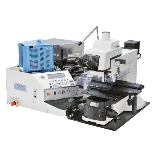
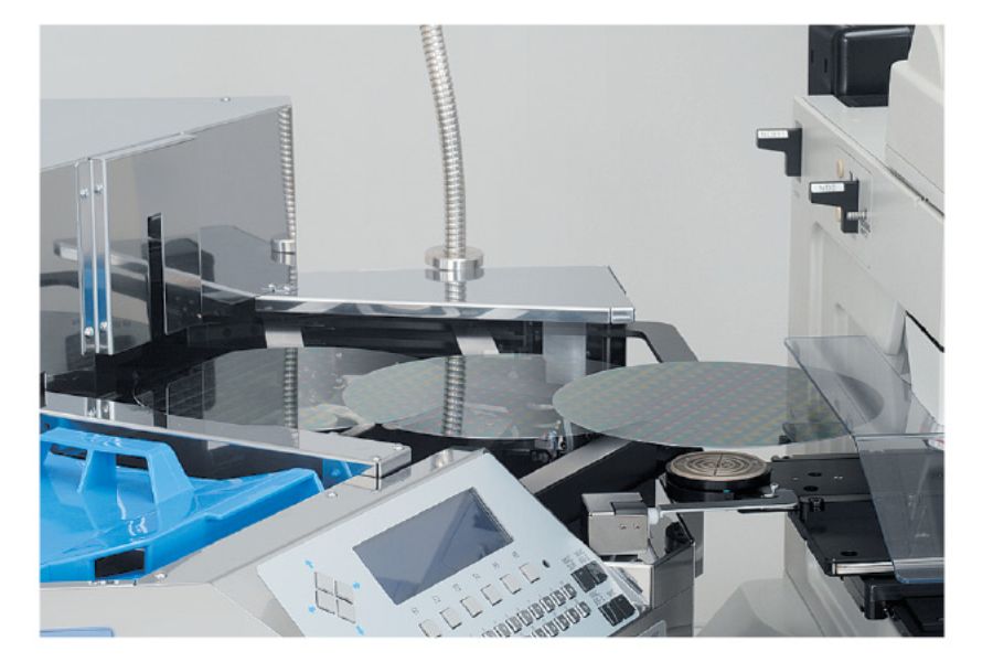
100µm Ultra-Thin Wafer Chuck
Chips are becoming ever thinner through advances in manufacturing, requiring handling of extremely thin wafers.
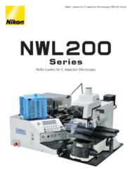
The NWL200 Series loads ultra-thin wafers to a thickness of 300µm and 200µm as standard, or 100µm as an option.