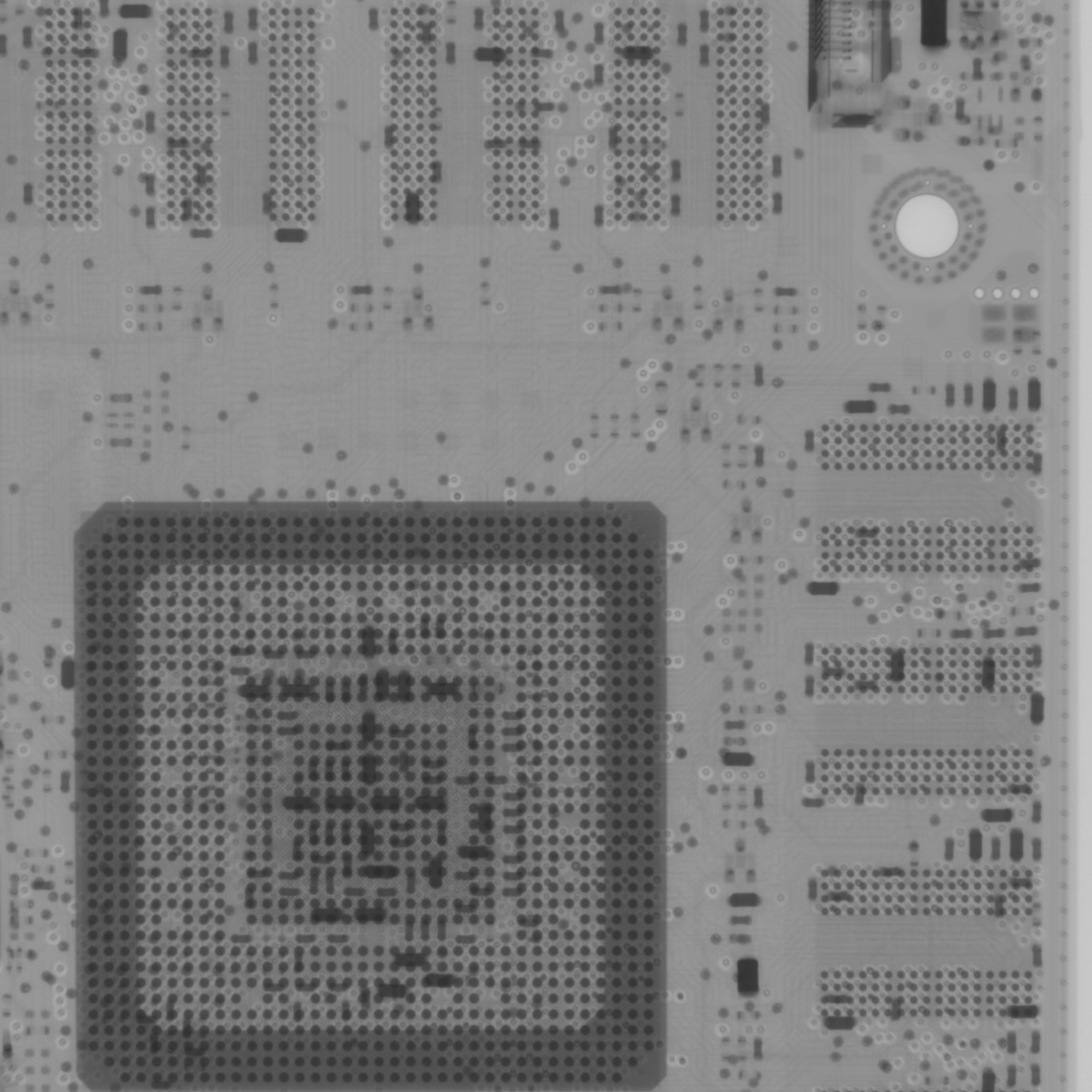
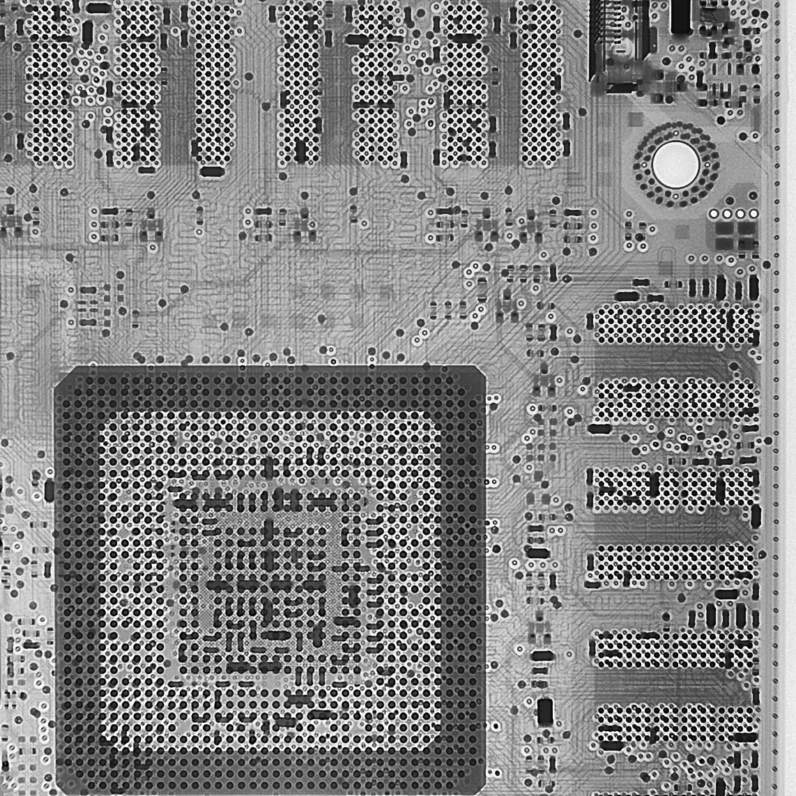
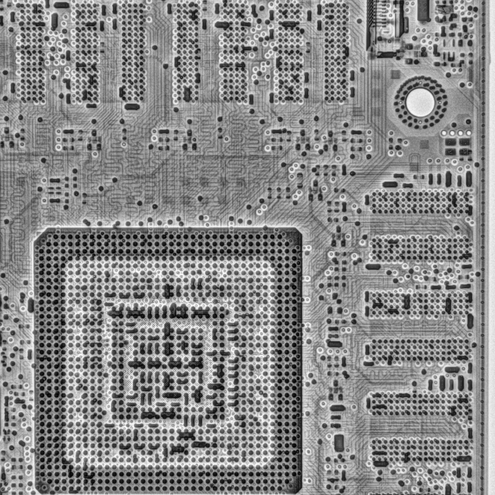
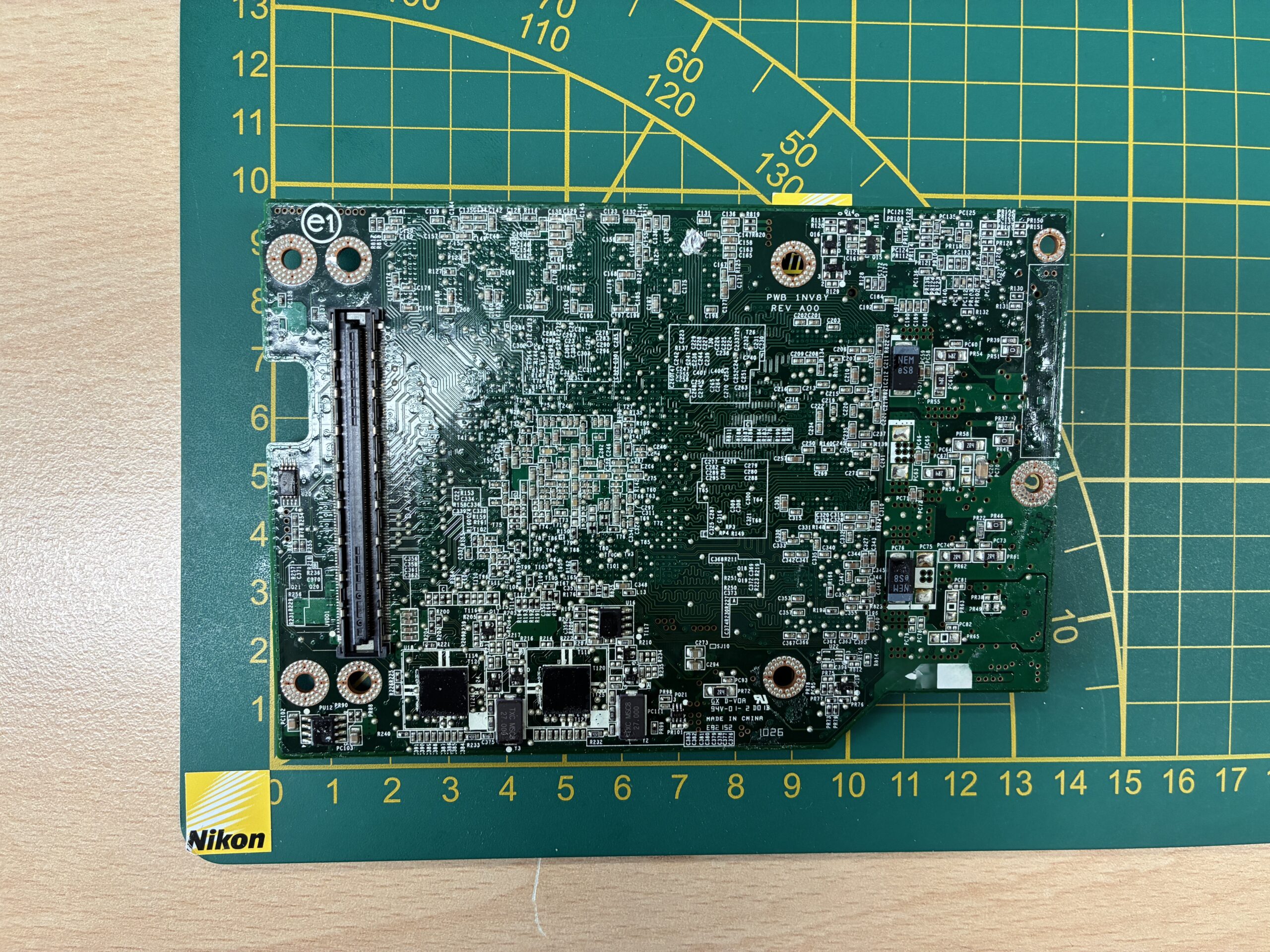
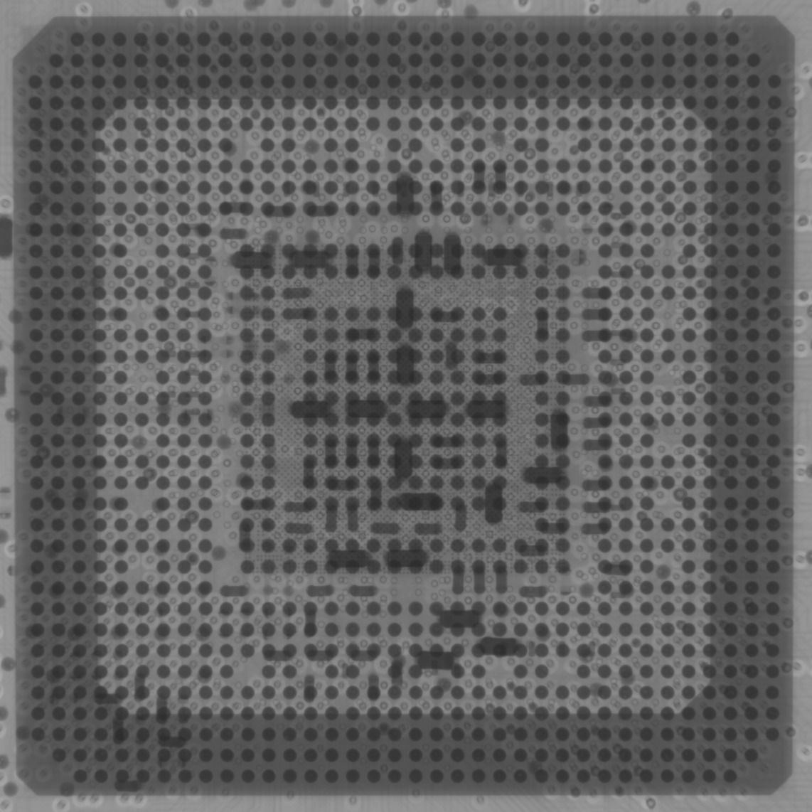
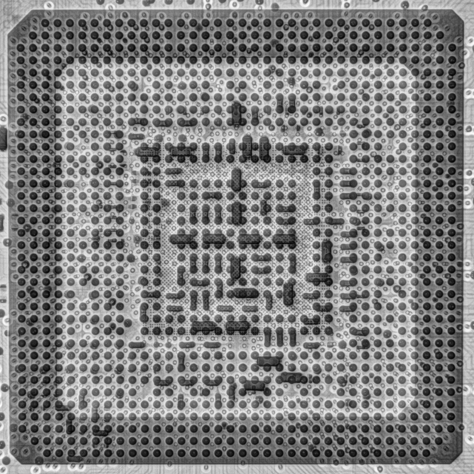
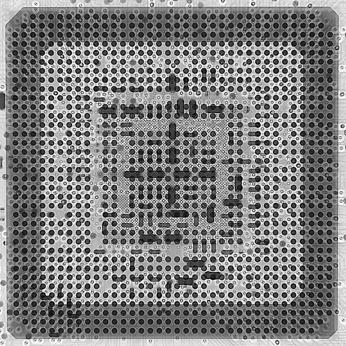
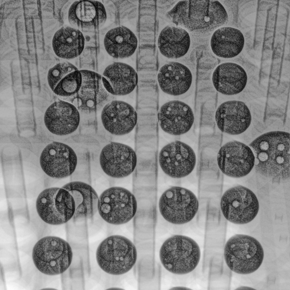
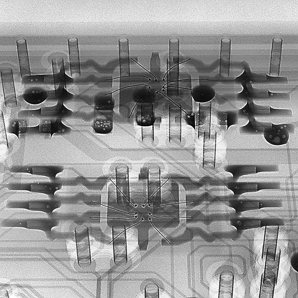
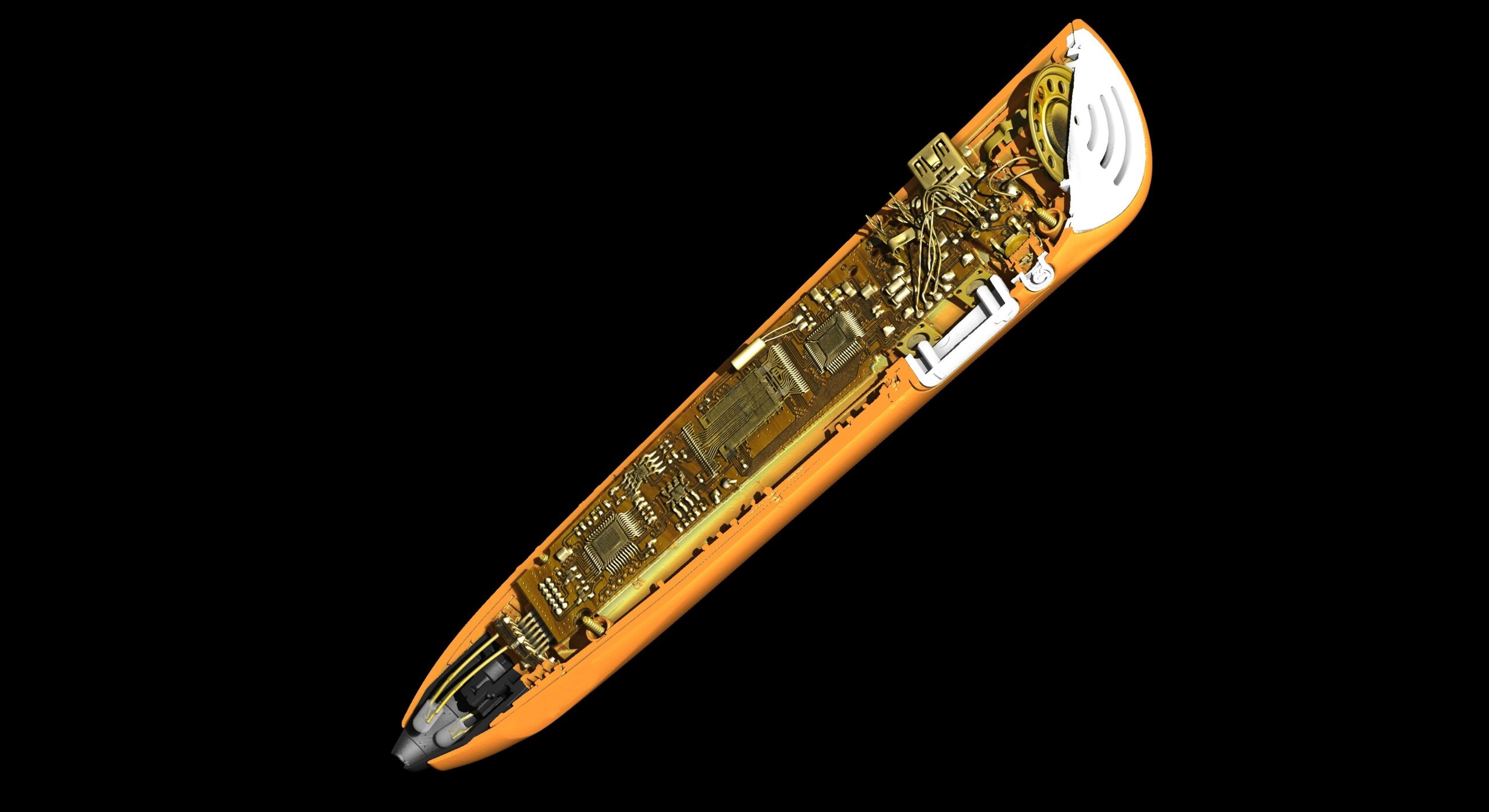
Each January, CES (Consumer Electronics Show) sets the tone for the year ahead in electronics innovation, showcasing ever more powerful, compact, and integrated technologies. Inspired by this global spotlight on advanced electronics, our Scan of the Month for January focuses on a laptop graphics card. As electronics continue to become smaller, denser, and more powerful, gaining visibility into their internal structures without damaging them is more critical than ever.
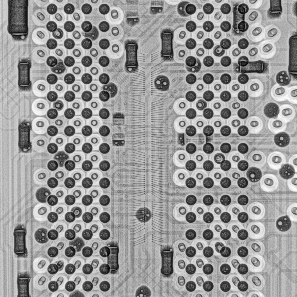
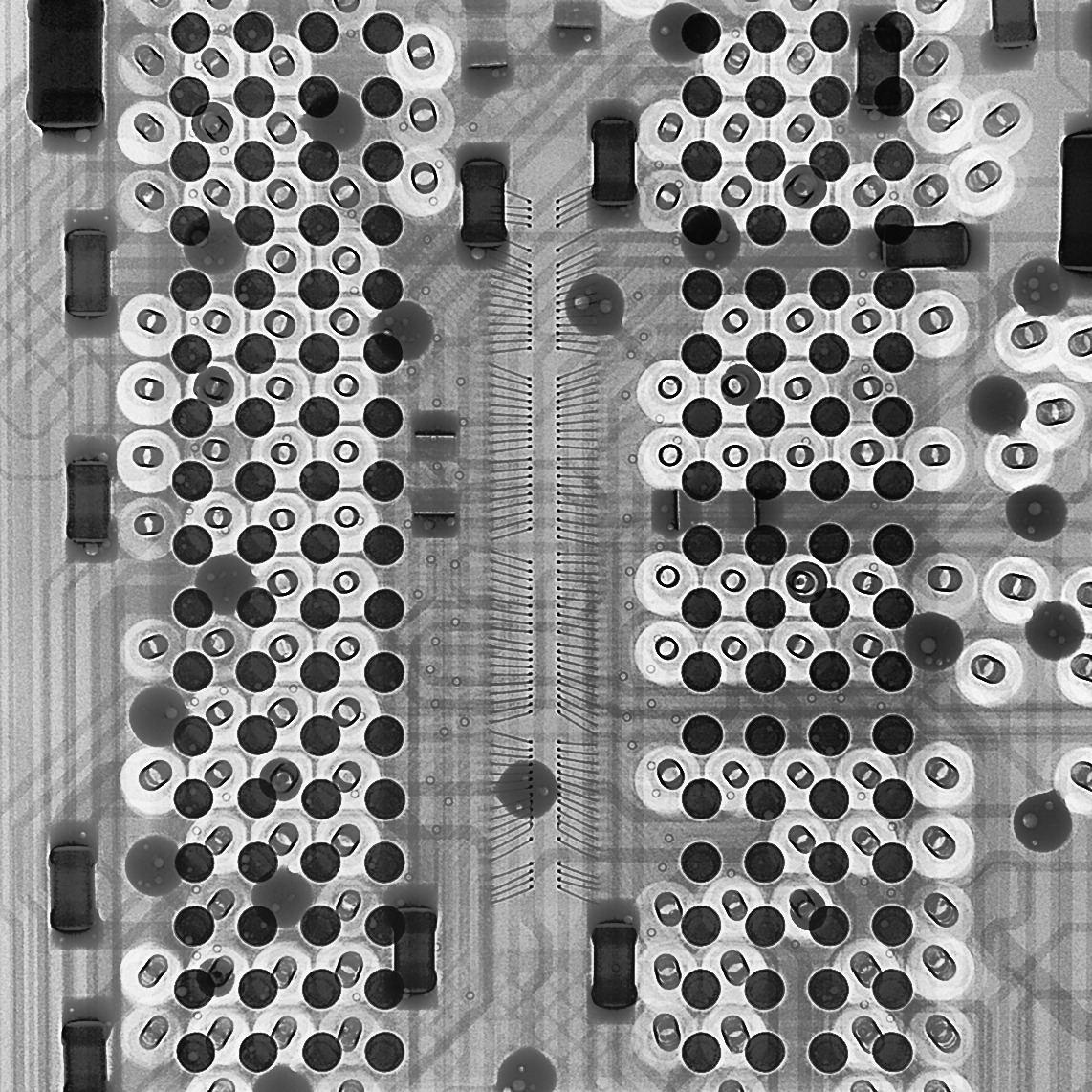
Sergei Kolobov, X-ray Application Engineer, leverages Nikon X-ray radiography, enhanced with High Contrast Filter 2.0, to reveal the hidden complexity inside this critical component. This scan of the month highlights the power of High Contrast Filter 2.0, a recent enhancement for Nikon’s XT V Series, designed to dramatically improve visibility when inspecting high-attenuation and mixed-density assemblies such as electronic boards.
Why X-ray radiography for electronics inspection?
While computed tomography (CT) is often associated with volumetric analysis, radiography remains a fast, powerful, and highly effective inspection technique especially for electronics where rapid feedback and high contrast are essential.
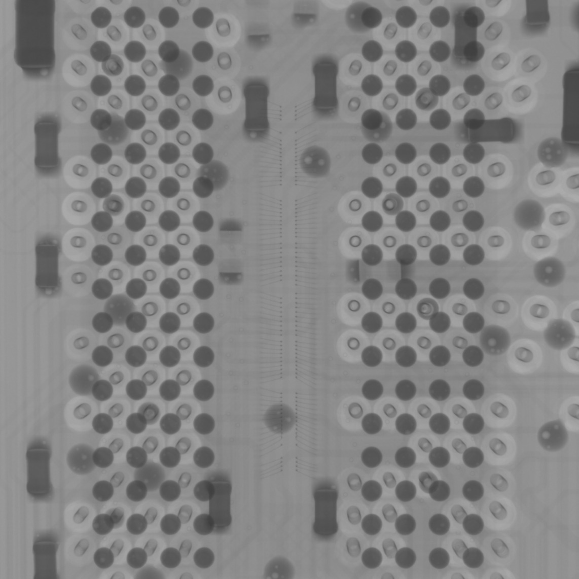
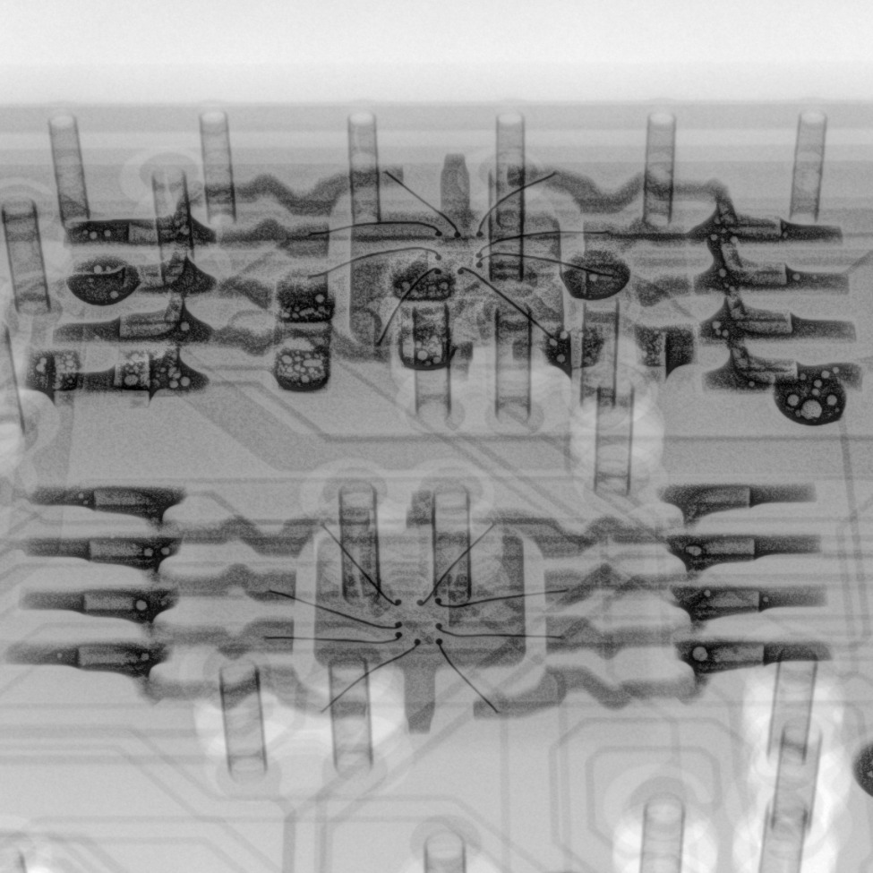
In this case, a series of high-quality radiographs was captured to examine:
- Component placement and alignment
- Solder joint consistency
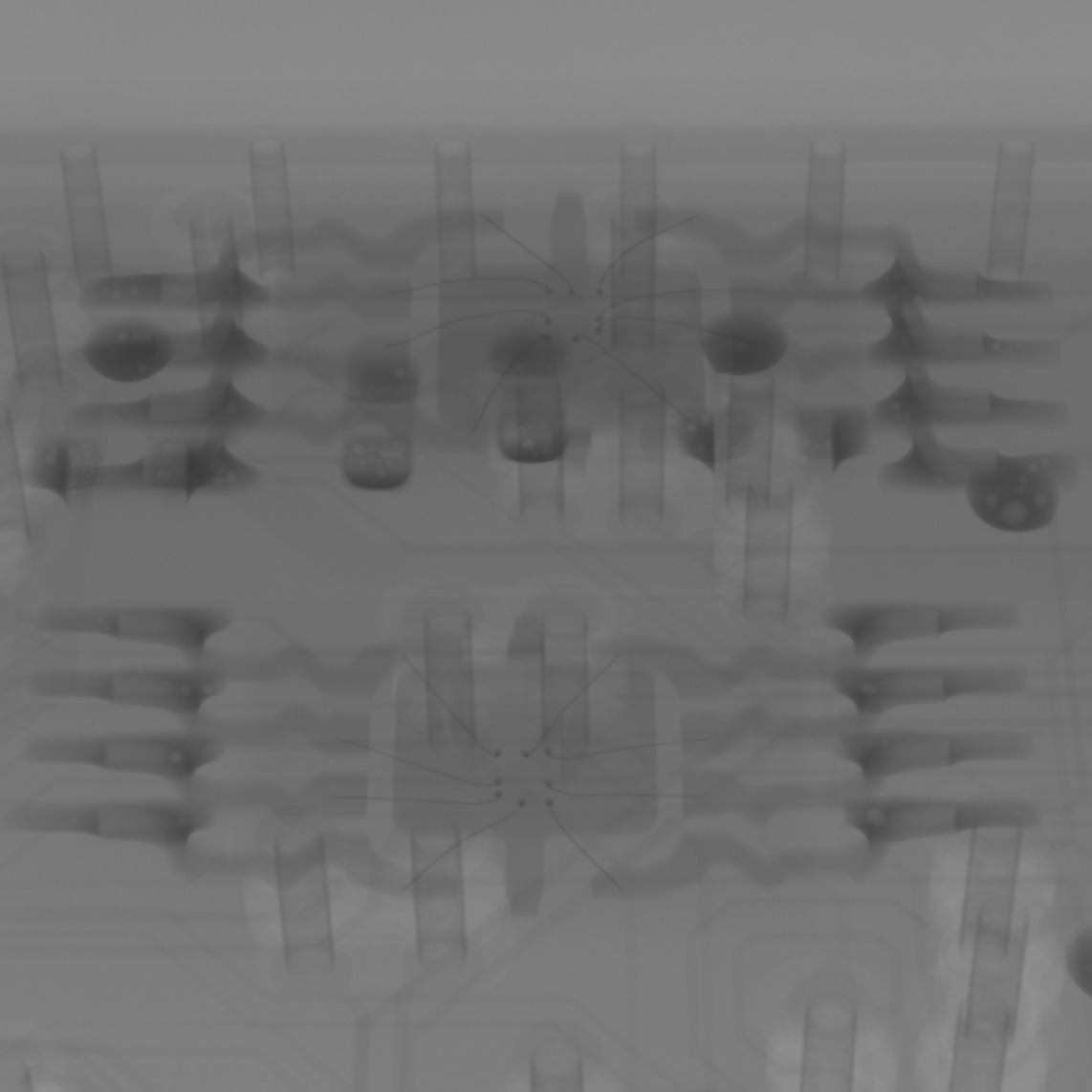
- Internal routing and layer stacking
- Power and signal paths within the PCB
- Dense metallic features and shielding elements
Enhancing Visibility with High Contrast Filter 2.0
Electronics assemblies such as graphics cards present a unique imaging challenge: highly attenuating materials (copper, solder, shielding) sit alongside low-contrast substrates and fine structures.
The scans were processed using High Contrast Filter 2.0, which significantly improves image clarity by:
- Enhancing contrast between materials with similar absorption levels
- Preserving fine details in both low- and high-density regions
- Reducing visual noise without masking critical features
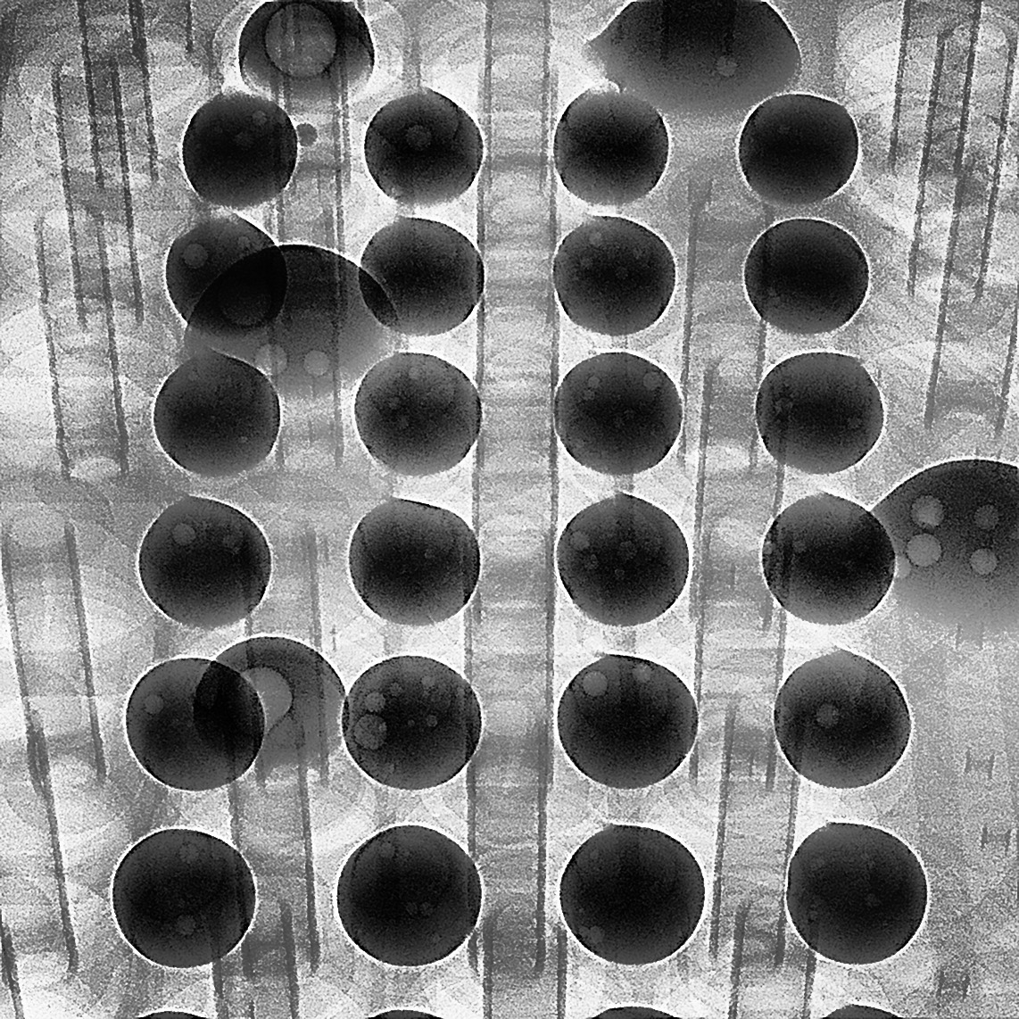
The result is a set of radiographs that clearly reveal subtle internal details such as solder distribution and internal traces while maintaining sharp definition across the entire field of view.
Technologies unveiled at CES increasingly rely on compact, high-performance electronic architectures where reliability and quality are paramount. From AI acceleration to advanced graphics and power management, these innovations demand inspection solutions capable of keeping pace with design complexity.
Nikon’s X-ray radiography, enhanced with High Contrast Filter 2.0, provides exactly this capability delivering fast, high-clarity insight into electronic assemblies without slowing development or production cycles.
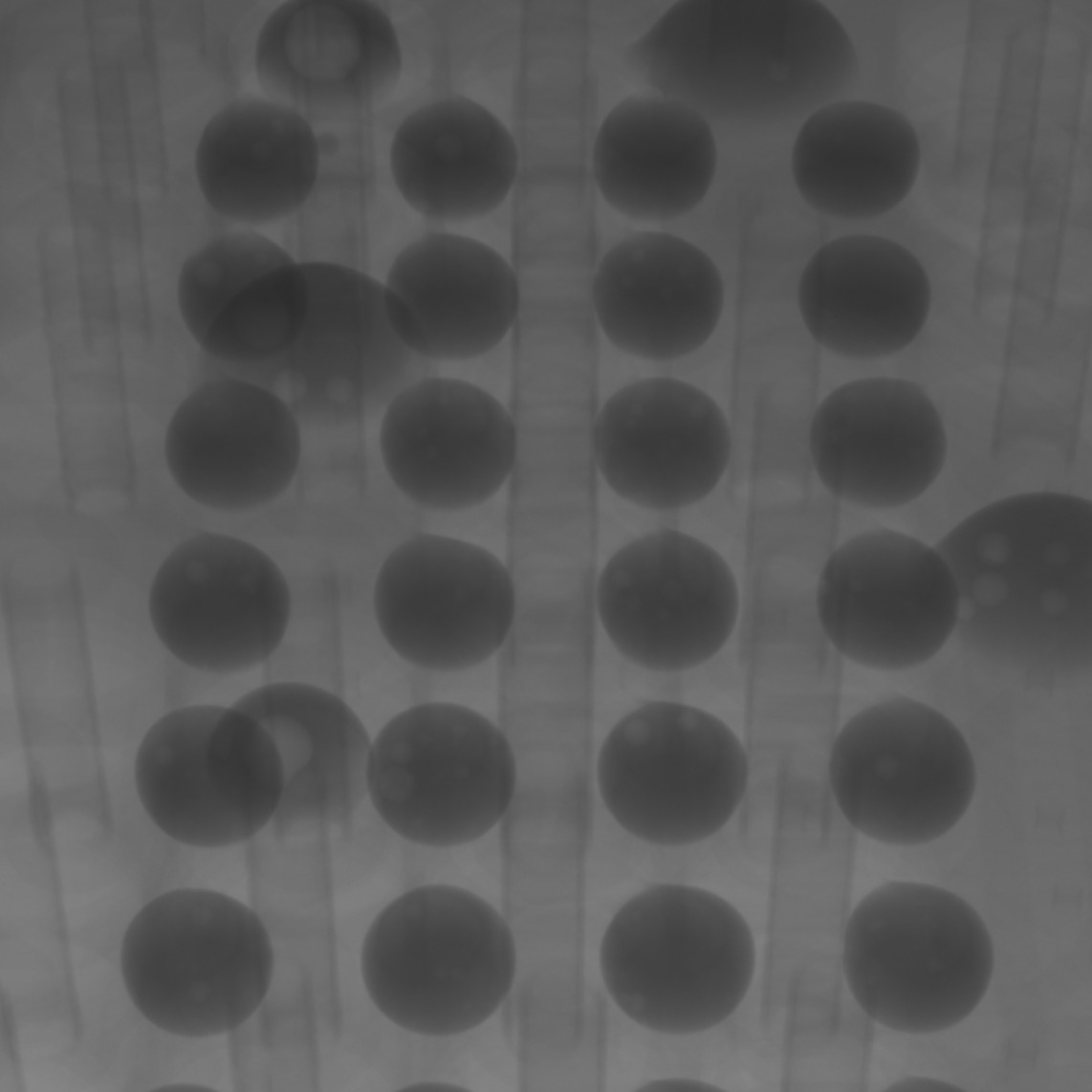
As a concrete example, High Contrast Filter 2.0 also reveals porosity that was previously difficult to detect. Defects that materially affect the part but were nearly invisible in earlier scans can now be clearly resolved:
2D Radiographs setup and technical details
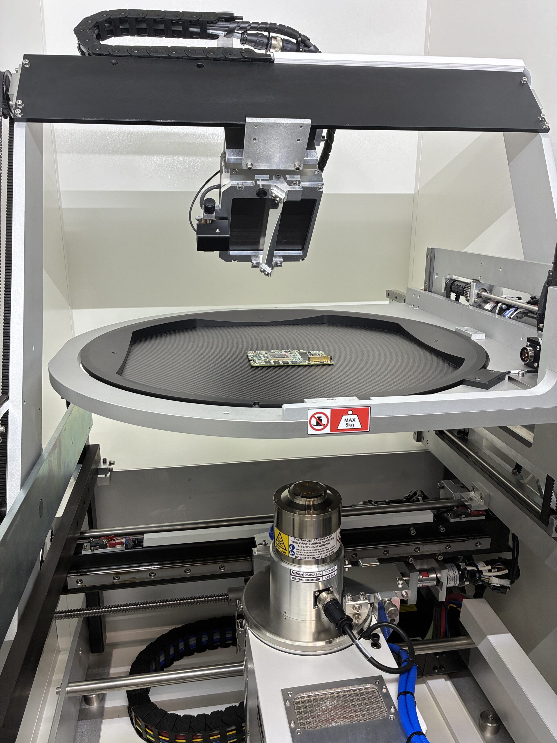
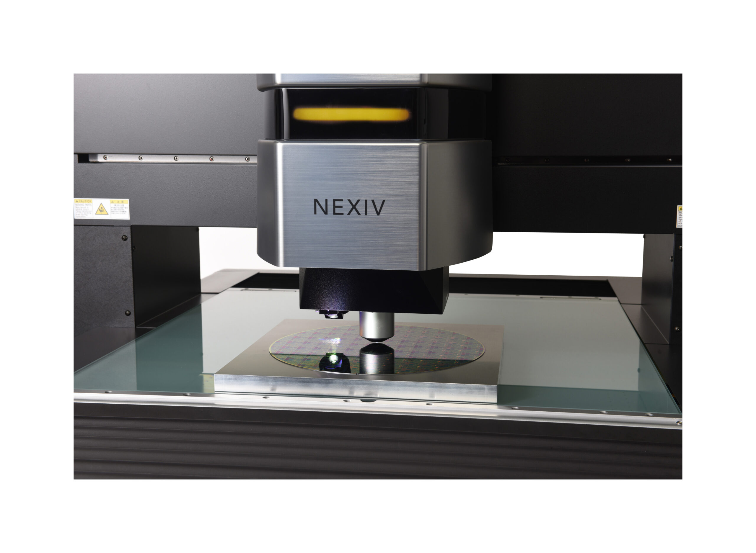
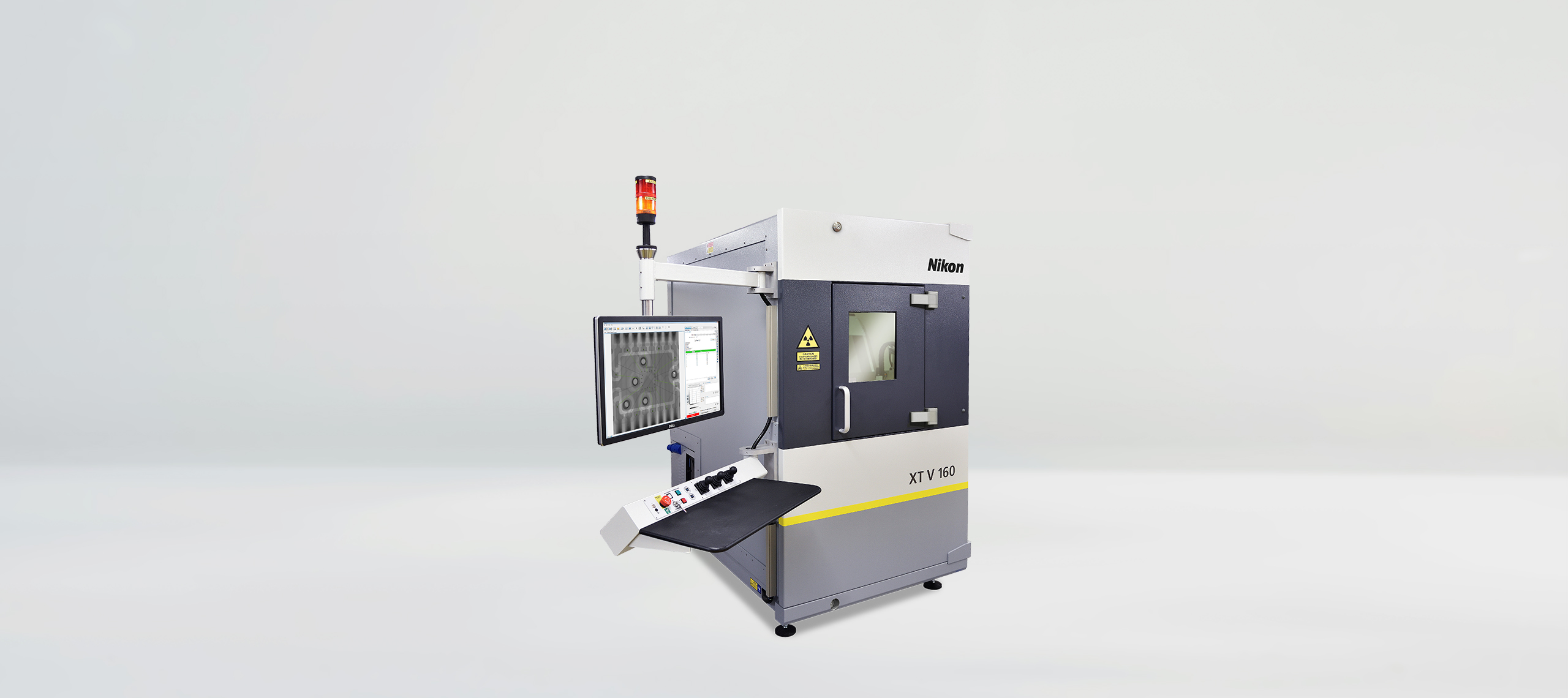
All images were acquired using a Nikon XT V 160 X-ray system, configured for high-contrast electronics inspection. The system was equipped with a 160 kV Xi transmission target X-ray source and a 1515 Dx detector, operating in radiography mode. Scan parameters were adjusted dynamically to optimize image quality, with X-ray voltage ranging between 130 and 160 kV and power levels between 3 W and 20 W. Depending on the inspection area and required resolution, image resolution varied from 0.4 to 60 microns, with exposure times between one and ten seconds. Each radiograph was acquired using one to ten frames, with no projections required, resulting in a total scan time of approximately five minutes for the complete inspection sequence.
Fast insight for complex electronics
This Scan of the Month highlights how Nikon’s XT V Series, combined with High Contrast Filter 2.0, enables fast, high-impact inspection of complex electronic assemblies using radiography alone. By enhancing visibility across challenging mixed-material structures, Nikon’s latest image processing innovations help manufacturers, researchers, and failure-analysis specialists extract maximum value from every scan, quickly, reliably, and non-destructively.
