Products and promotions may differ based on your selected region.
Scatter Correction CT: improves X-ray scan image quality
New level of QualityMeasurementSpeed
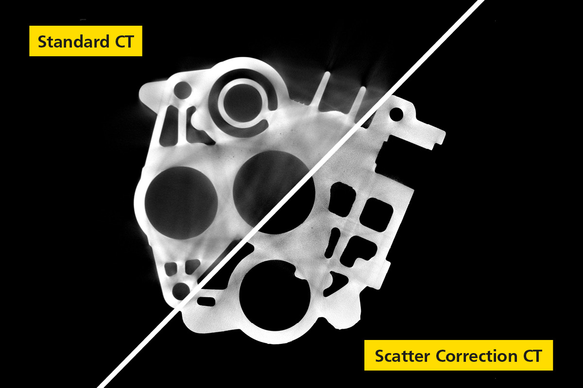
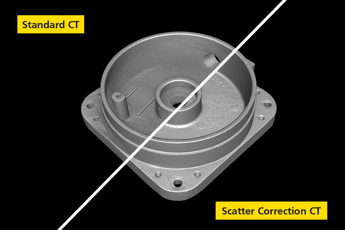
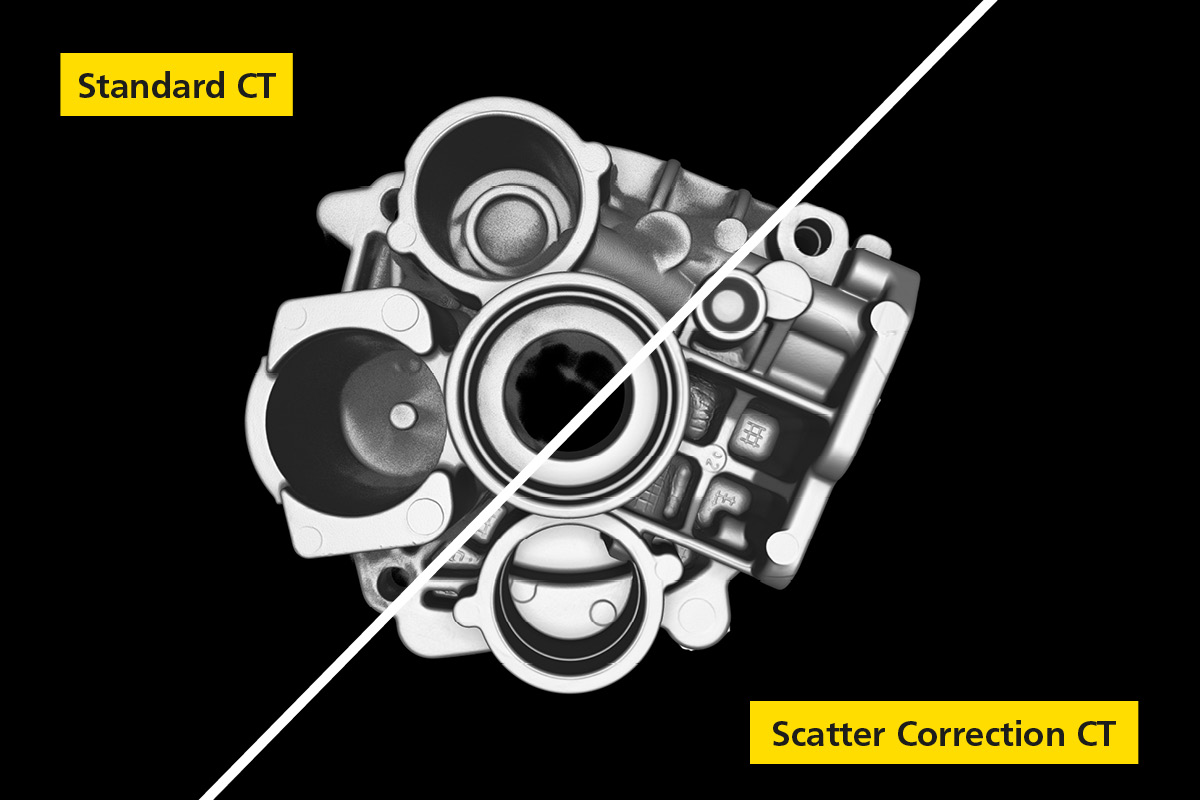
Nikon’s Scatter Correction CT enhances traditional industrial CT scanning by employing advanced physics-based modelling to correct for X-ray scatter artifacts. Designed to improve image quality and ease of measurement, Scatter Correction CT empowers users to visualise and analyse dense materials with unprecedented clarity and accuracy.
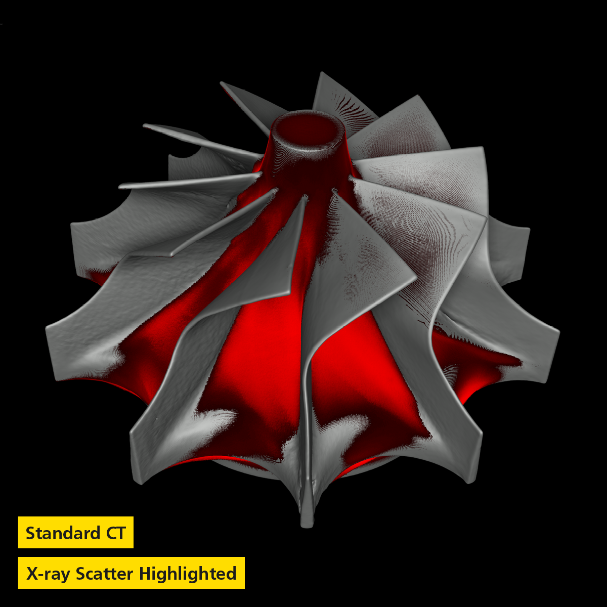
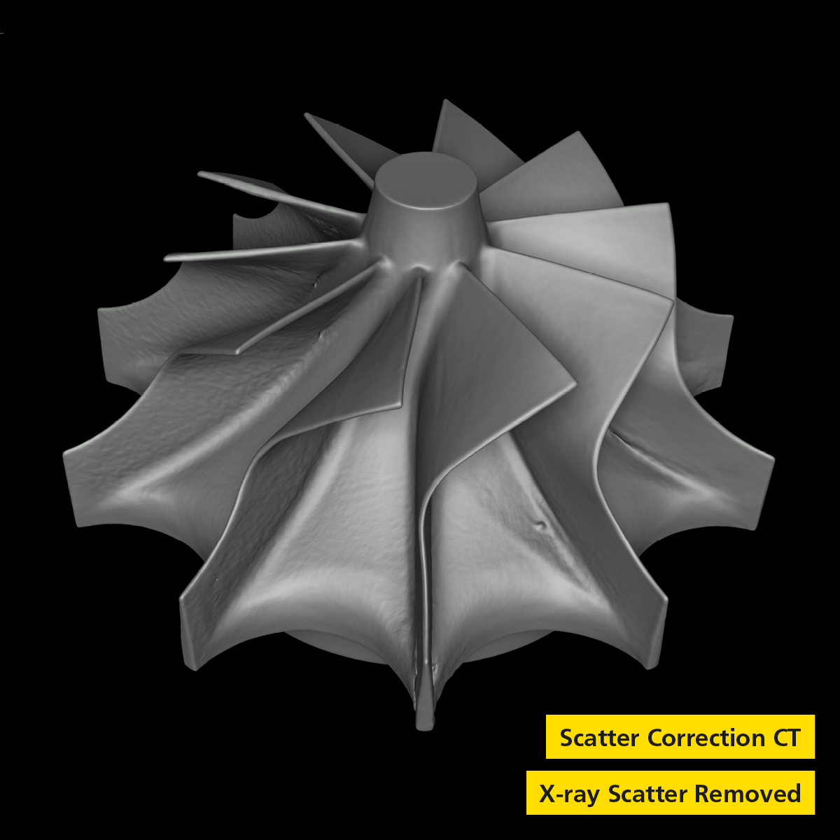
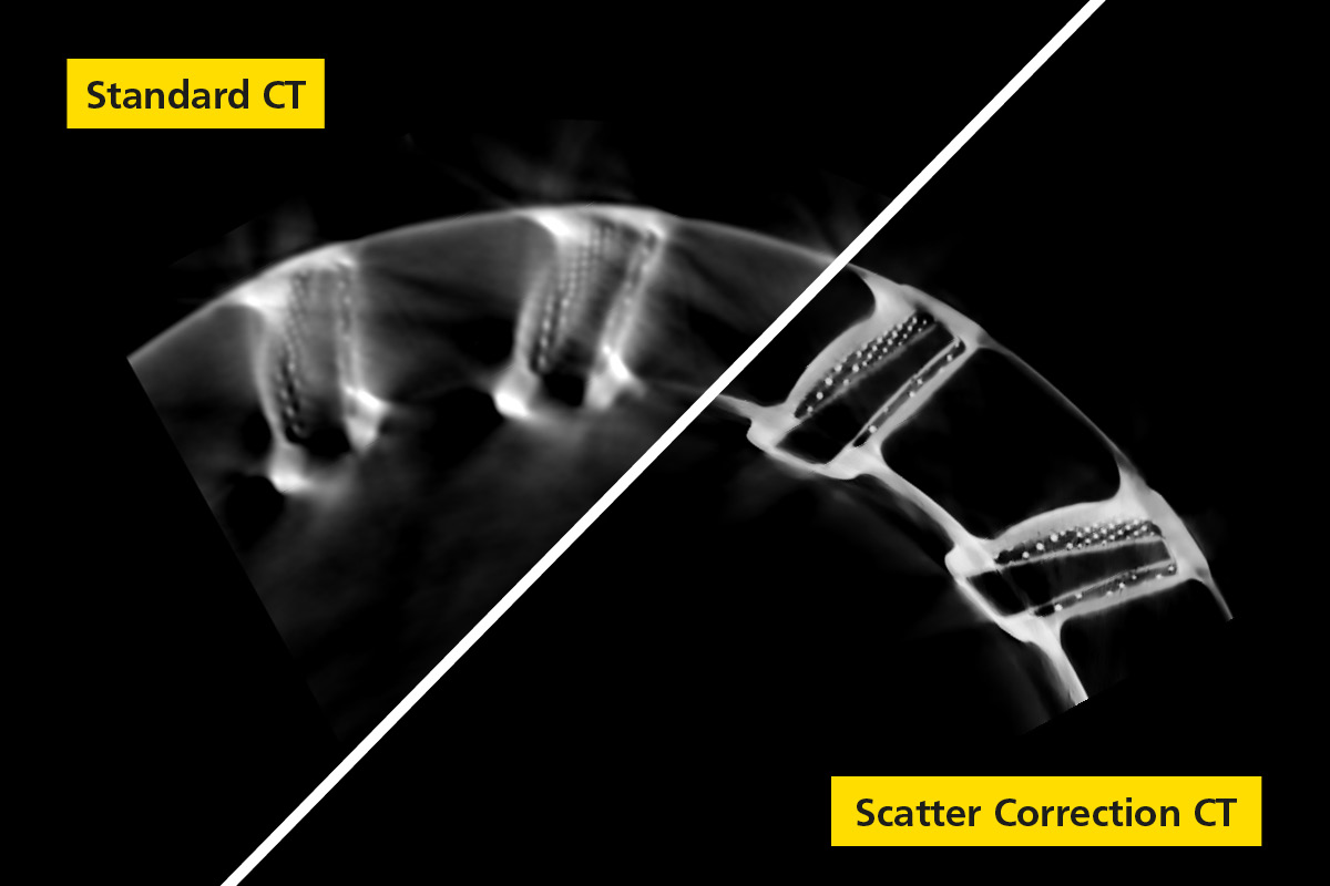
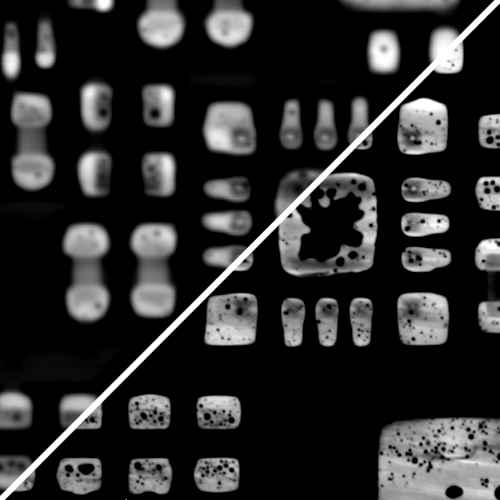
By addressing the challenges posed by X-ray scatter — including cloudy haloes, false inhomogeneities, and edge blurring — Scatter Correction CT enables users to uncover previously obscured defects and details. At the same time, the correction dramatically reduces scan times compared to traditional 2D CT methods, allowing a significantly faster and more efficient inspection.
Product Highlights
Enhanced image quality
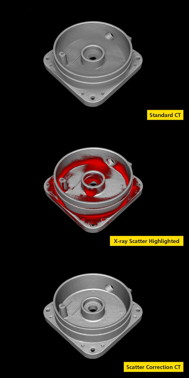
Scatter Correction CT enables precise measurement and inspection of objects that suffer from the disruptive effects of X-ray scatter. By removing the presence of cloudy haloes, false inhomogeneities and edge blurring, material surfaces can be confidently determined, and previously occluded fine details can be resolved.
Significantly faster scan times
For complete component inspection, Scatter Correction CT achieves scan times more than 100 times faster than traditional 2D CT methods using line detectors, which can take tens of hours to acquire a complete scan of a single component. This dramatic reduction in scan time allows manufacturers to significantly increase their inspection throughput and accelerate their quality control processes.
Exceptionally easy to use
Scatter Correction CT is seamlessly built into the scanning workflow and requires just a single click to enable it, making it exceptionally simple for the operator to use. This user-friendly approach streamlines the scanning process, reduces the need for specialised skills, and improves overall productivity in industrial CT scanning applications.
Expanded application options
Scatter Correction CT is available across all Nikon X-ray sources and systems in the 225 kV and above range and is fully compatible with all Nikon CT scanning acquisition modes, providing a versatile solution for diverse industrial applications. By correcting for scatter artifacts in dense materials including aluminium, steel, ceramic, and Inconel, Scatter Correction CT opens up new opportunities for non-destructive testing and metrology across various industries.
Enhanced surface determination and inspection accuracy
Scatter Correction CT significantly reduces X-ray scatter artifacts in 3D CT data, enabling precise surface determination and consistent inspection results. This improvement in data quality enhances volume analyses and internal and external measurements. As a result, Scatter Correction CT allows for reliable measurements that were previously challenging or impossible to perform accurately.
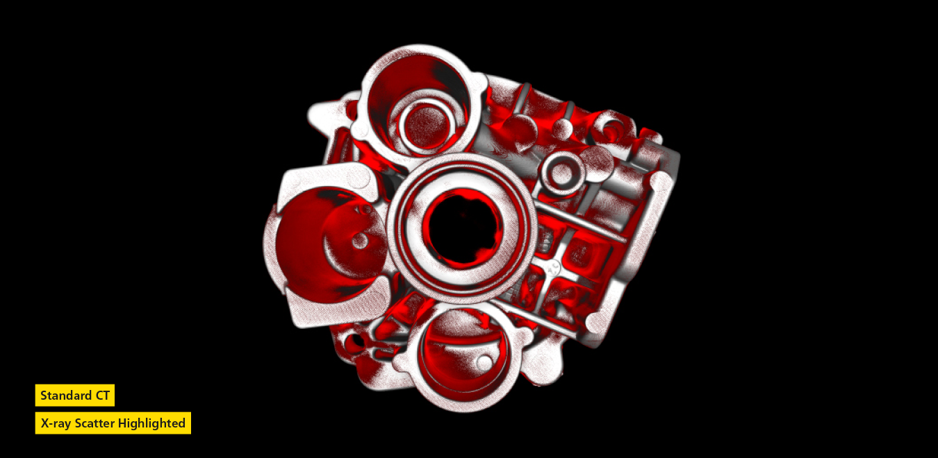
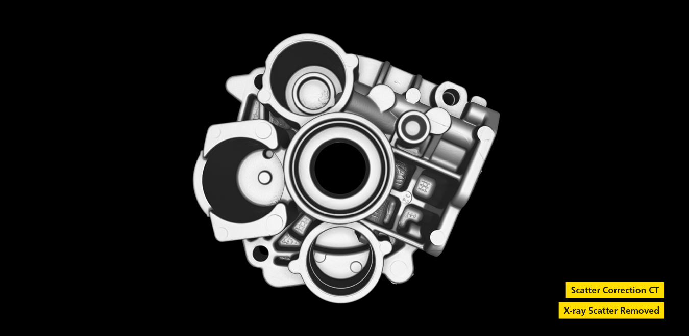
Industry Applications
Automotive

As the automotive industry races ahead, embracing cutting-edge technologies, the need for efficient and accurate quality control has never been greater. Scatter Correction CT steps up to the challenge, offering a rapid and reliable solution for inspecting complex automotive components like engine parts and transmission systems. By significantly reducing scan times compared to traditional 2D CT methods, Scatter Correction CT empowers automotive manufacturers to keep pace with production demands while ensuring the highest quality and reliability standards.
Batteries

The booming battery and electrification sector demands robust inspection methods to guarantee the performance and safety of battery cells. Scatter Correction CT provides battery manufacturers with an invaluable tool, enabling them to non-destructively examine the internal structure of battery cells and spot potential flaws or irregularities. By offering clear and accurate images of the cell’s internal components, Scatter Correction CT empowers manufacturers to streamline their production processes, boost battery performance, and minimise the risk of safety hazards, ultimately contributing to the development of more reliable and efficient energy storage solutions.
Aerospace

In the highly regulated aerospace industry, Scatter Correction CT delivers an unparalleled level of precision for non-destructive testing. By minimising X-ray scatter artifacts in materials like aluminium and Inconel, this advanced technology enables accurate measurement of both external and internal structures with exceptional clarity, ensuring the highest quality standards in aerospace component manufacture.
Metals
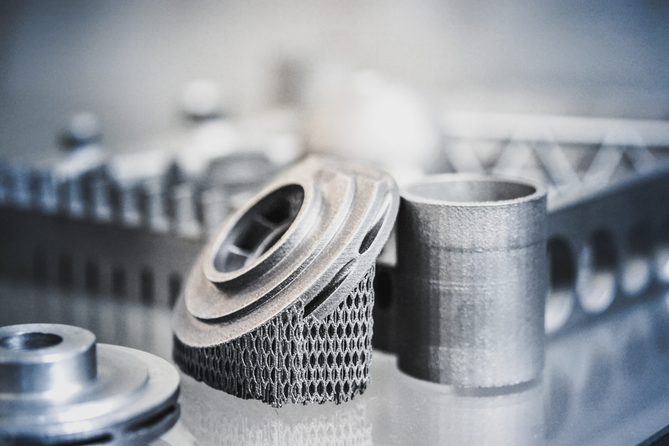
Metals are the backbone of many industrial sectors, from castings to machined components and cutting-edge additive manufacturing. Scatter Correction CT offers a powerful solution for examining metal parts with unprecedented detail. This technology enhances analysis capabilities by employing advanced physics-based modelling to correct X-ray scatter artifacts. It addresses challenges posed by dense materials like aluminium, steel, and Inconel, eliminating cloudy haloes, false inhomogeneities, and edge blurring. As a result, manufacturers can more effectively visualise and analyse components, improving image quality and measurement accuracy.
Academic Research

In the academic sector, scientists analyse a vast spectrum of materials and structures, from geological wonders and fossilised remains to next generation composites and alloys. Scatter Correction CT offers researchers a versatile tool, empowering them to non-destructively investigate the structure of these diverse samples with exceptional clarity and precision. By providing high-resolution images and accurate measurement capabilities, Scatter Correction CT unlocks a greater level of understanding and fuels knowledge growth across various scientific disciplines.
FAQs
Scatter Correction CT is particularly effective for scanning dense materials such as aluminium, steel, ceramic, and Inconel. Due to the presence of scatter artifacts, these materials often prove challenging for traditional CT scanning methods. By correcting these artifacts, Scatter Correction CT enables accurate inspection and analysis of numerous components and structures across various industries, including aerospace, automotive, and additive manufacturing.
Scatter Correction CT offers a significant advantage in terms of scan time when compared to traditional scatter-free 2D CT methods using line detectors. For comprehensive component inspection, Scatter Correction CT achieves scan times more than 100 times faster than these traditional methods, which can take tens of hours to acquire a complete scan or a single component. This dramatic reduction in scan time allows manufacturers to significantly increase throughput and accelerate their quality control processes.
Scatter Correction CT is widely available and highly compatible with Nikon’s X-ray CT systems. The correction is available across all Nikon X-ray sources and systems in the 225kV and above range. Additionally, it can be combined with all Nikon CT scanning acquisition modes, including Circular CT, Helical CT, Half.Turn CT, Offset.CT, Pixel Split CT, and Panel Shift.
Scatter Correction CT employs advanced physics-based modelling to simulate and correct the interaction of X-rays with different materials. By removing cloudy haloes, false grey scale value (GSV) inhomogeneities, and edge blurring caused by X-ray scatter artifacts, Scatter Correction CT significantly enhances image quality. This improvement enables more precise visualisation and definition of fine details, defects, and surfaces, facilitating more accurate inspection and metrology.
One of Scatter Correction CT’s key advantages is its ease of use and minimal operator training requirements. The correction is seamlessly integrated into the scanning workflow and requires only a single click to enable it, making it exceptionally simple for operators to use. This user-friendly approach streamlines the scanning process, reduces the need for specialised skills, and improves overall productivity in industrial CT scanning applications.
Related Products
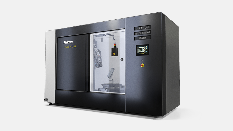
VOXLS 30 Series X-ray and CT Systems
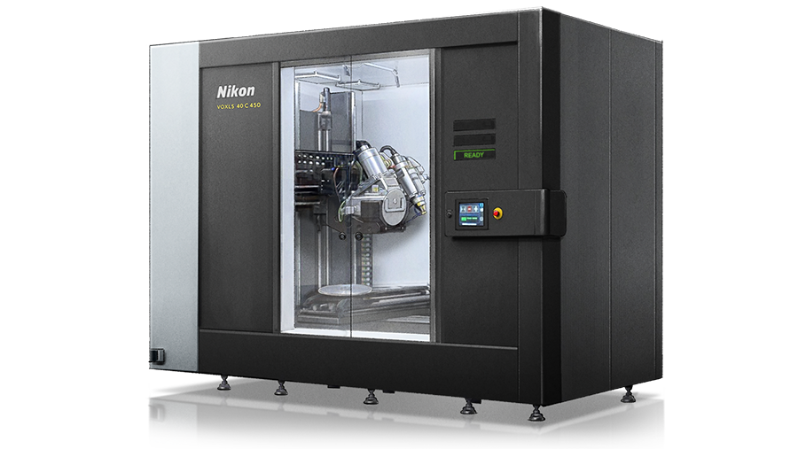
Configurable Large Envelope X-ray and CT Systems
Speak To Us About This Product
If you would like further details on this product or a more in-depth description, our expert team will provide you with additional information and, if required, arrange an on-site visit.
Talk to us in detail about your project and our experts will advise you on the best inspection system to meet your requirements.
Please fill out the form opposite and we will get in touch with you shortly.
