


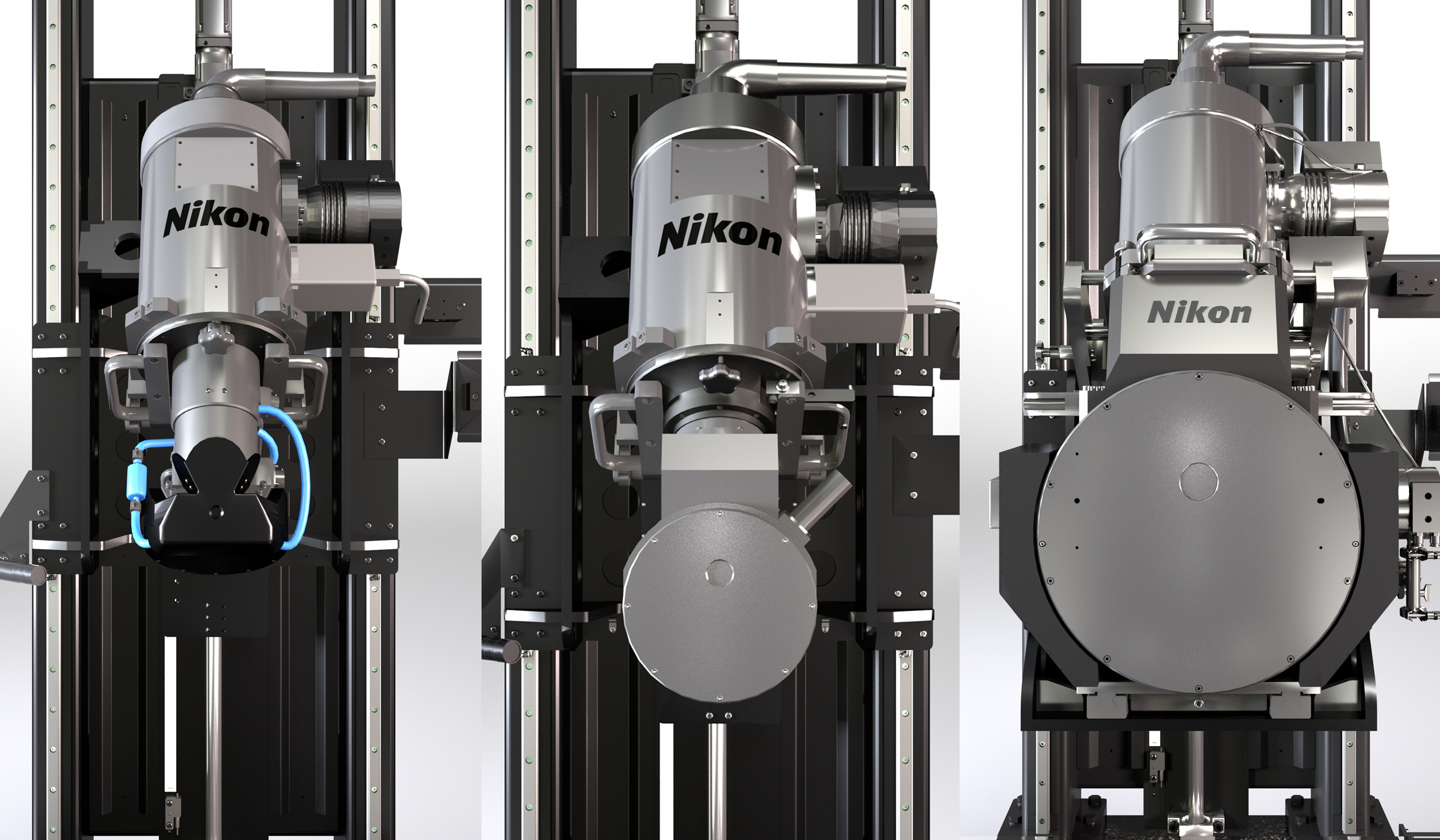
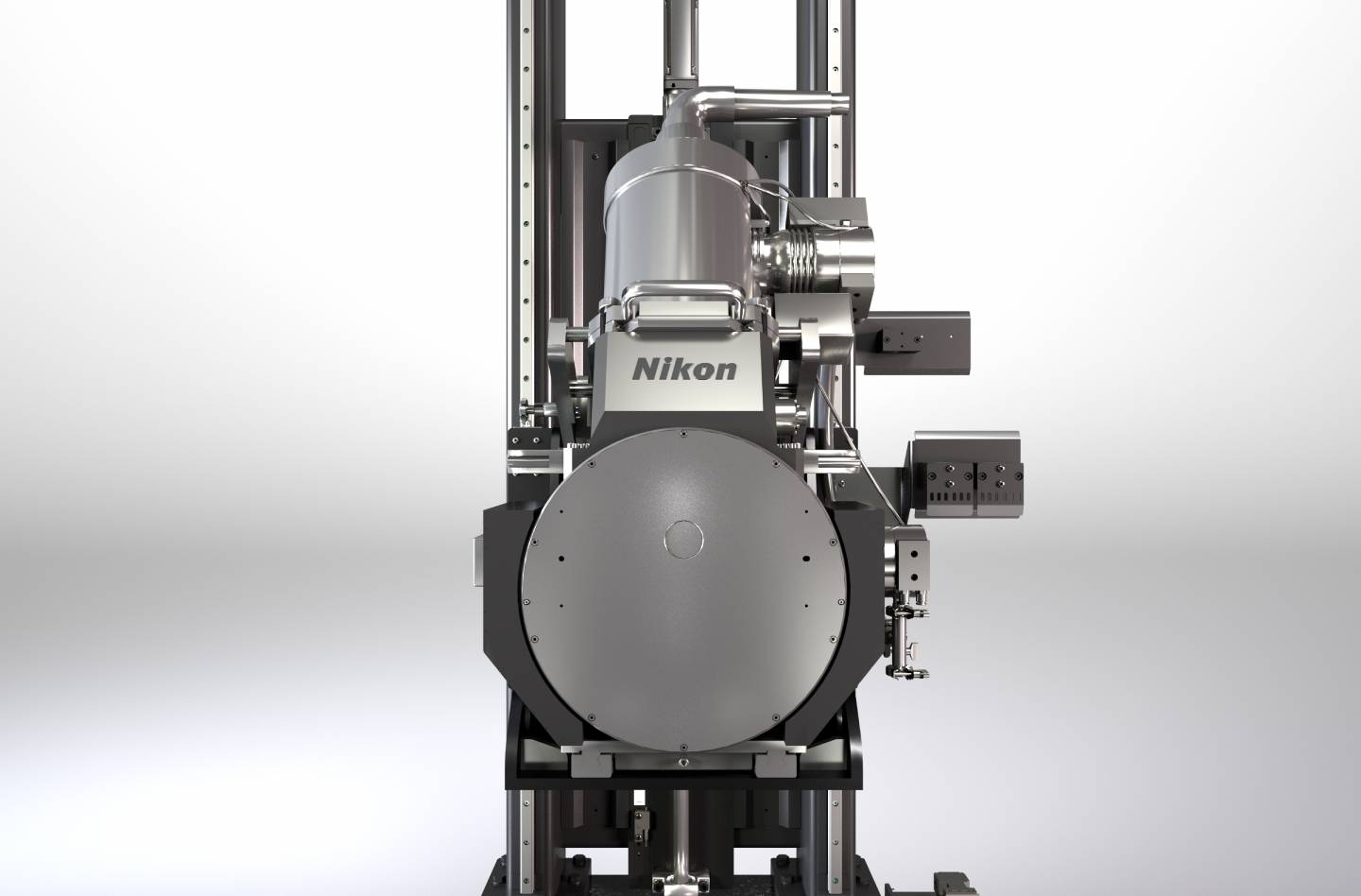
Unique 225 kV Rotating.Target 2.0
3-times greater power density provides faster scans and a better signal to noise ratio without loss of resolution. Advanced cooling technology enables continuous operation even at 450 W full power.

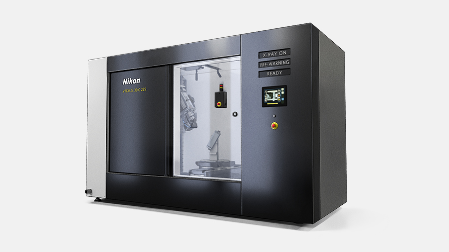
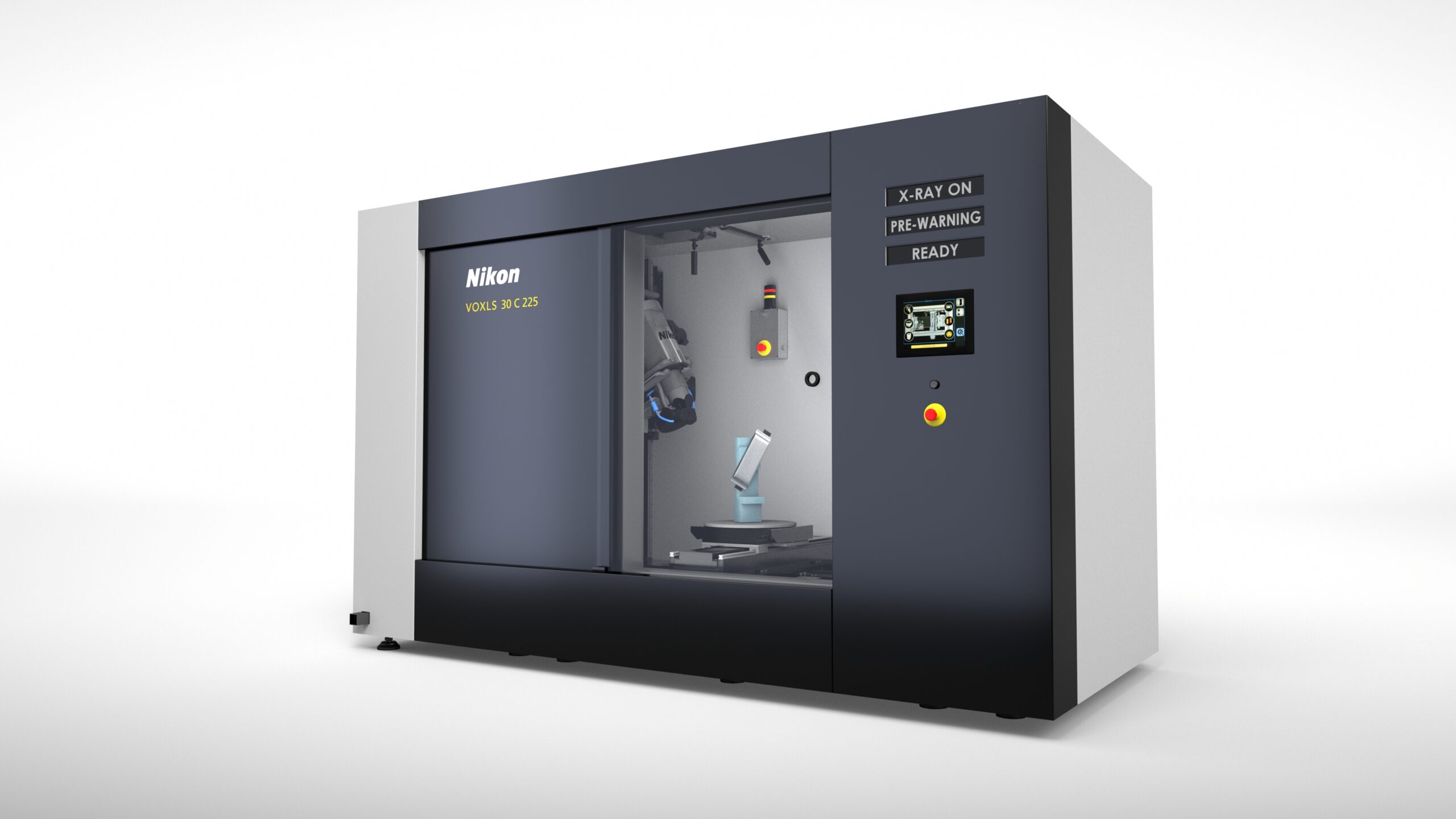
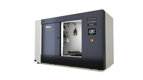
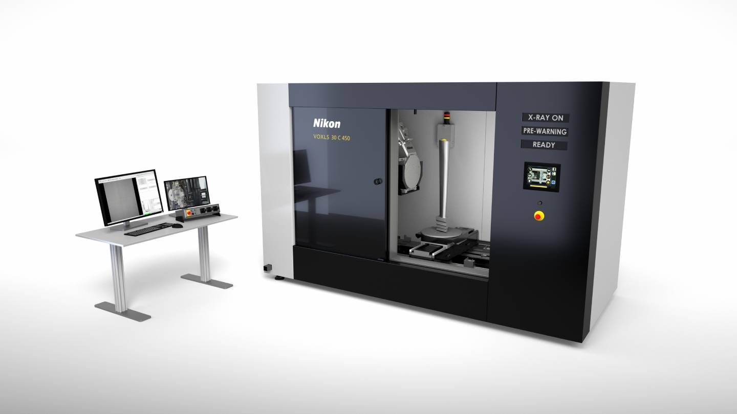
Nikon’s VOXLS 30 Series systems deliver automation readiness, packaged in an efficient footprint and paired with scan energies of 225 kV, 320 kV or 450 kV, making it an ideal solution for samples of low-to-high density.
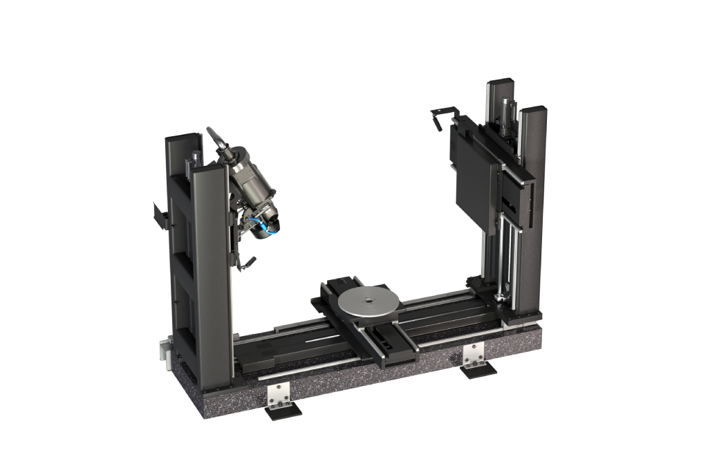
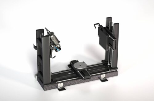
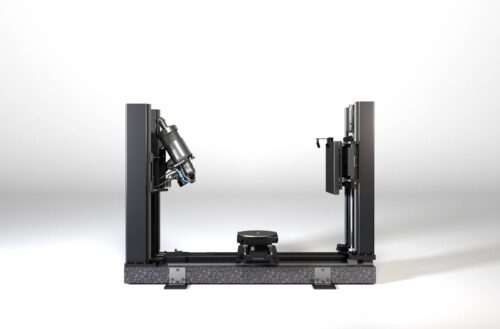
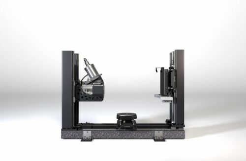
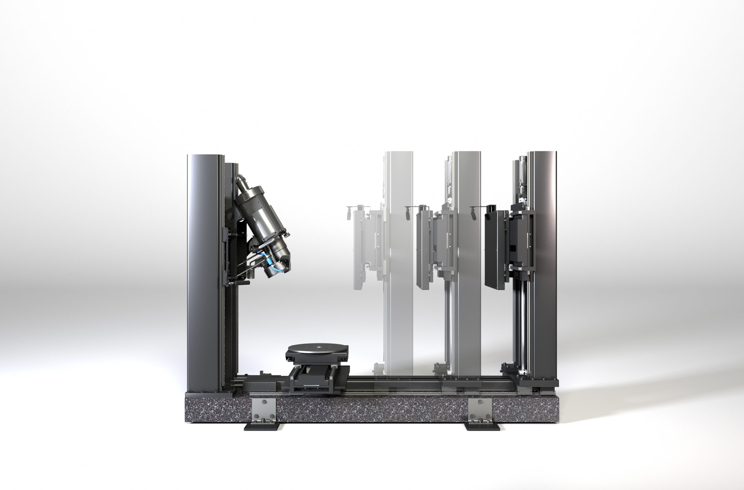
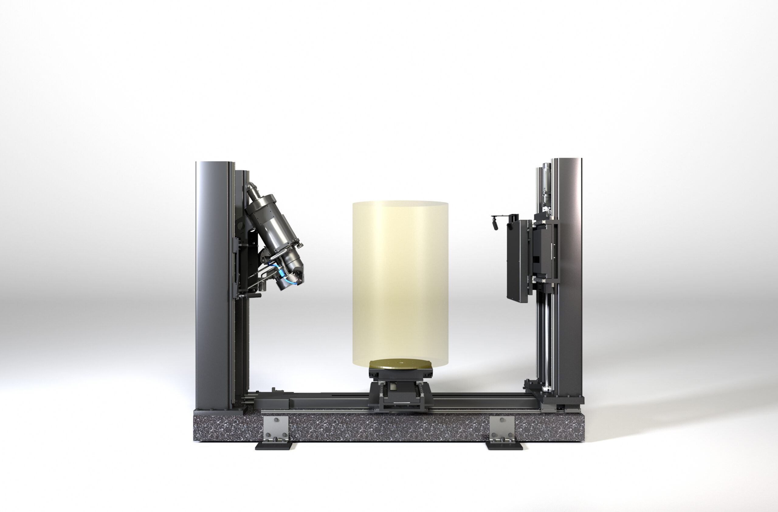
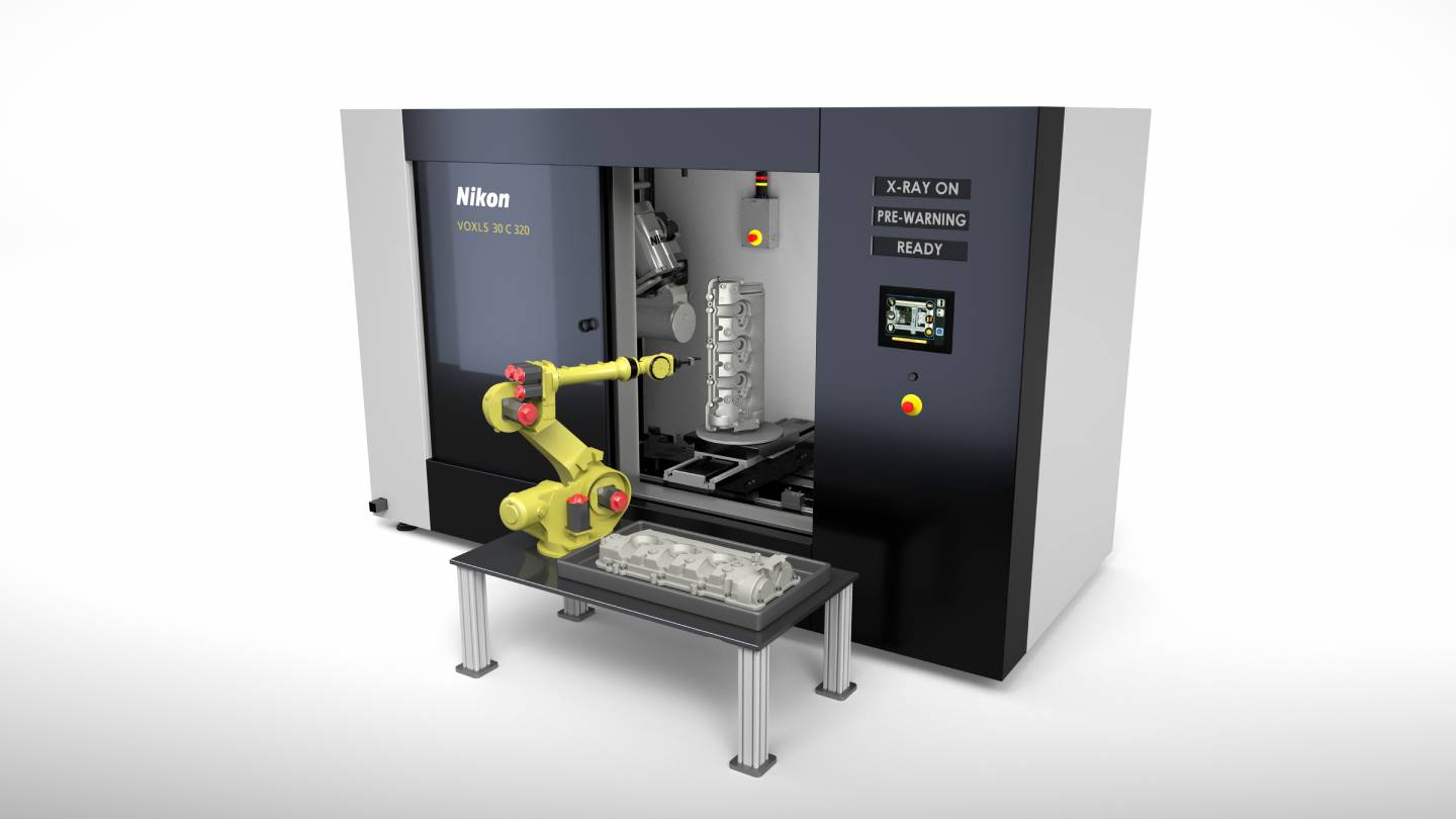
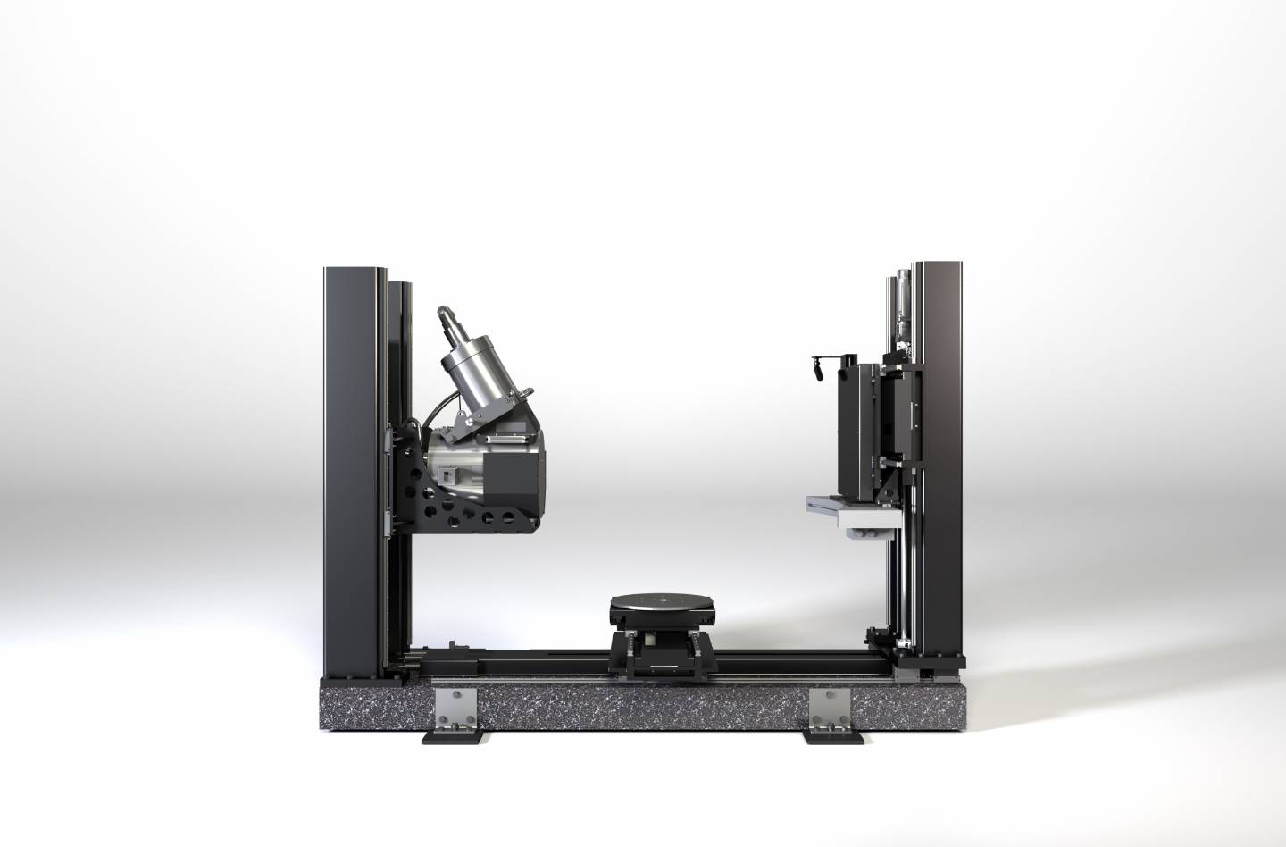
The VOXLS 30 Series of X-ray and CT systems is equally at home in the R&D laboratory as it is on the production line and can utilise automated robotics and industry 4.0 integrations. The system is built for repeatability and reliability through the metrology-grade, granite-based manipulator, and rigid steel towers.
Nikon’s VOXLS 30 C 225, 30 C 320 and 30 C 450 models have maximum source energies of 225 kV, 320 kV and 450 kV respectively for examining parts of various densities and sizes. By offering a selection of thoughtfully designed sources, Nikon empowers manufacturers to configure the optimal inspection system for their quality control needs. The flexible 30 Series scales to meet current and future requirements across diverse industries and sample types.
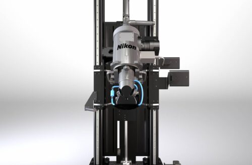
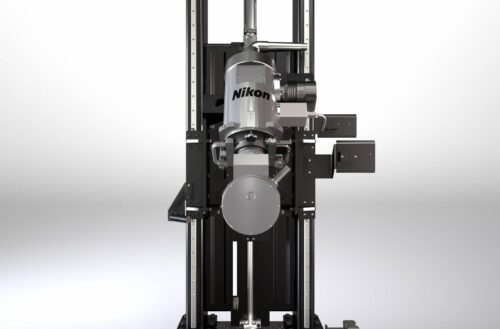
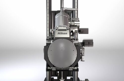
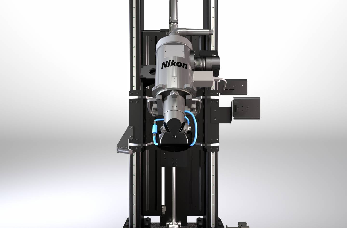
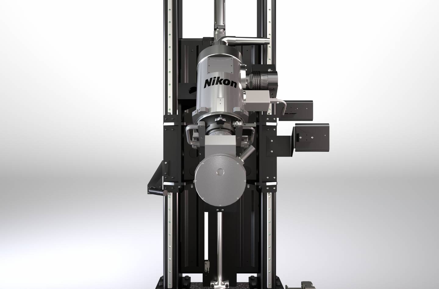
In traditional X-ray CT systems, the Focus to Imager Distance (FID) is either fixed or manually adjustable. However, the VOXLS 30 Series has motorised FID, allowing effortless adjustment of the distance between the X-ray source and detector with sub-millimetre precision. Reducing the FID provides dramatically greater X-ray photon flux, significantly faster scan times and increased signal-to-noise ratio for enhanced image quality.
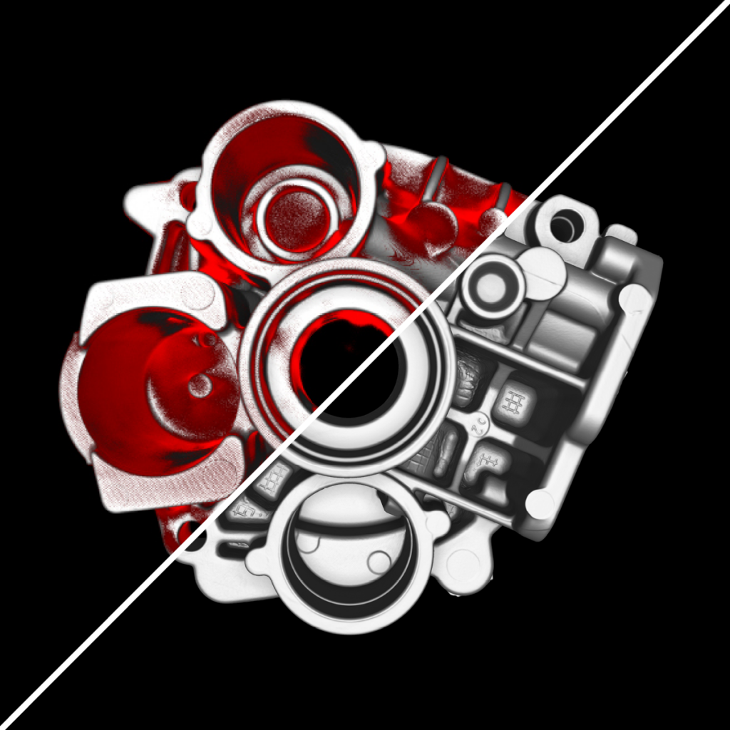
The VOXLS 30 Series can scan larger and more irregular-shaped parts thanks to Nikon’s wide range of scan envelope enhancement acquisition modes. These include X.Tend Helical CT, Panel Shift and Pixel Split CT, which are typically only available or compatible with larger X-ray CT systems.
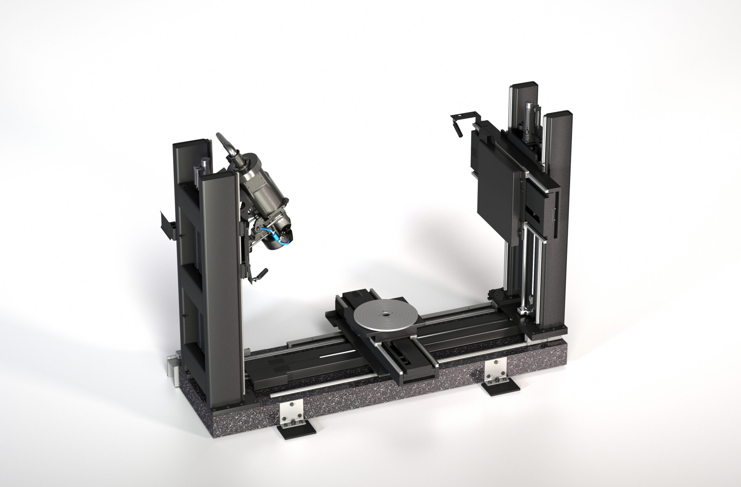
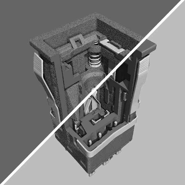
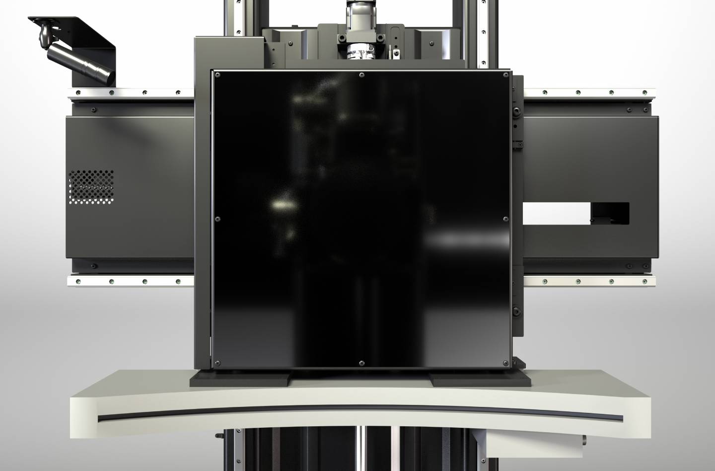
At the core of VOXLS 30 Series systems is a metrology-grade, granite-based manipulator coupled with rigid steel towers, high-precision motors and linear encoders. The resulting construction provides superior mechanical and thermal stability, enabling more accurate manipulator positioning and generating highly precise, repeatable measurement data throughout the entire scan volume.
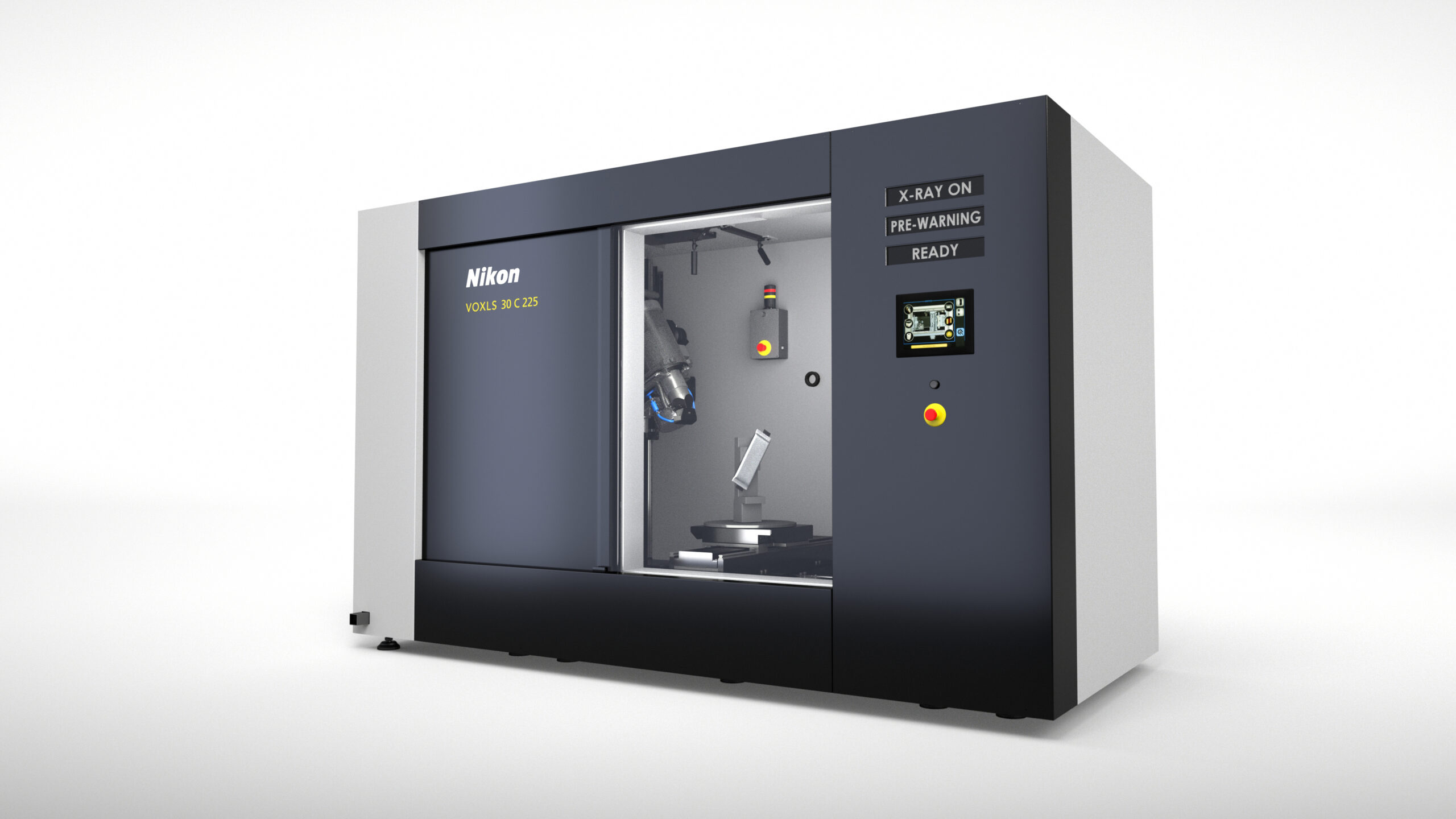
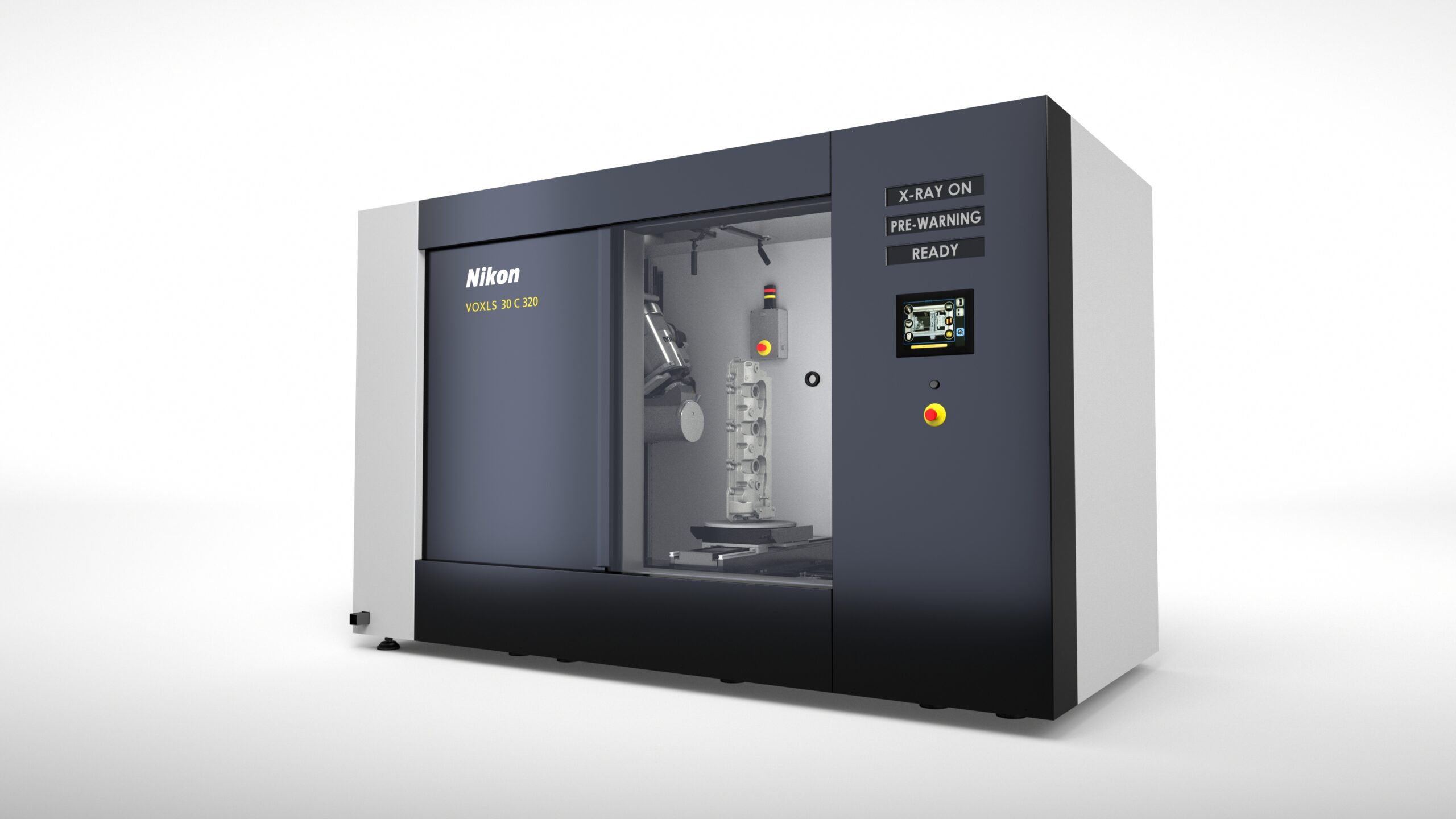
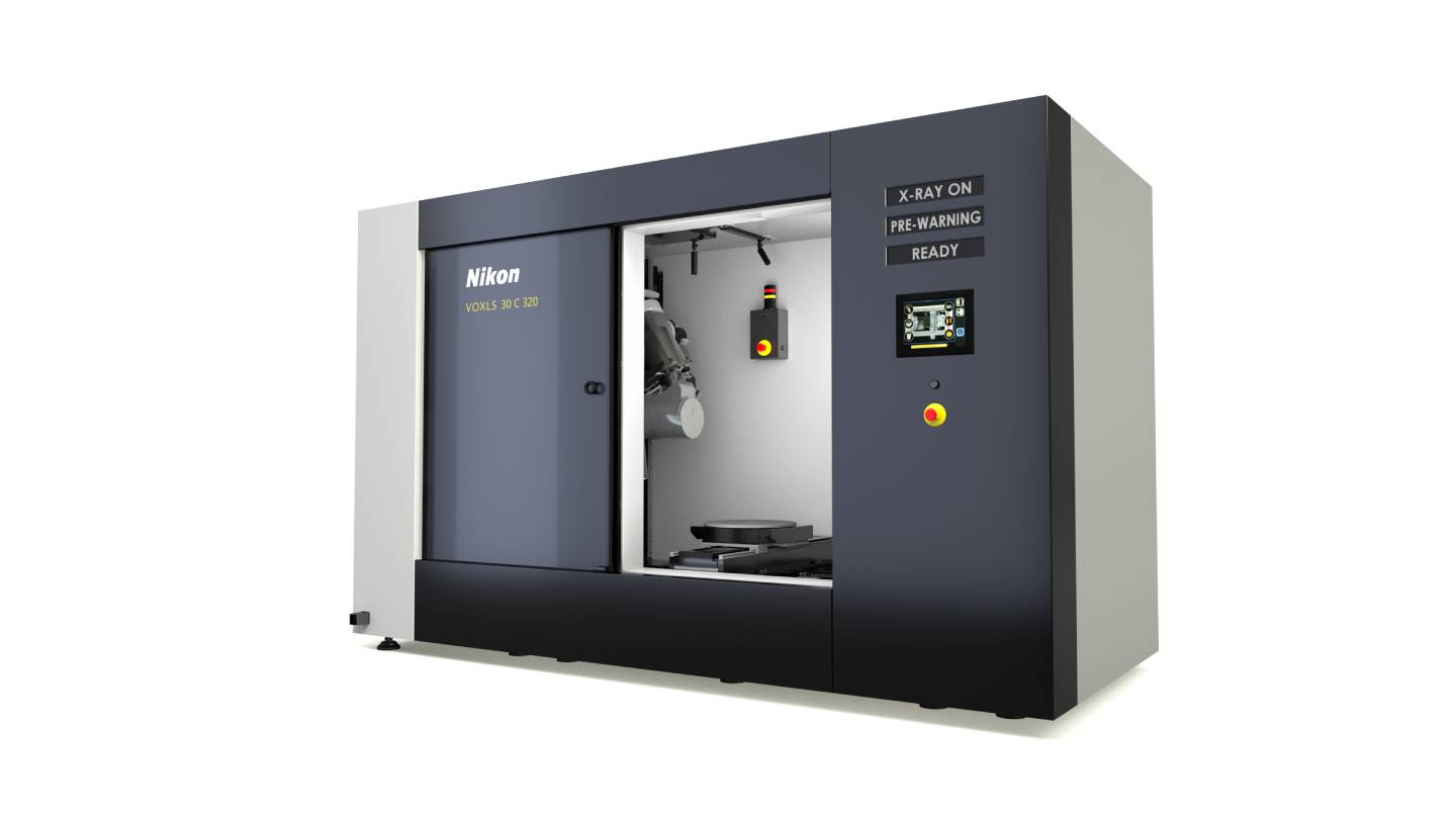
All VOXLS 30 Series systems come with a 1.3-metre-tall glass outer door with manipulator interlock, which gives the operator unrivalled visibility into the enclosure for precise and confident positioning of the scan object. This removes the need for light curtains and minimises the risk of sample collision with the X-ray sources and detectors. Two internal video cameras provide an excellent view even with the inner radiation safety doors shut and X-rays on.
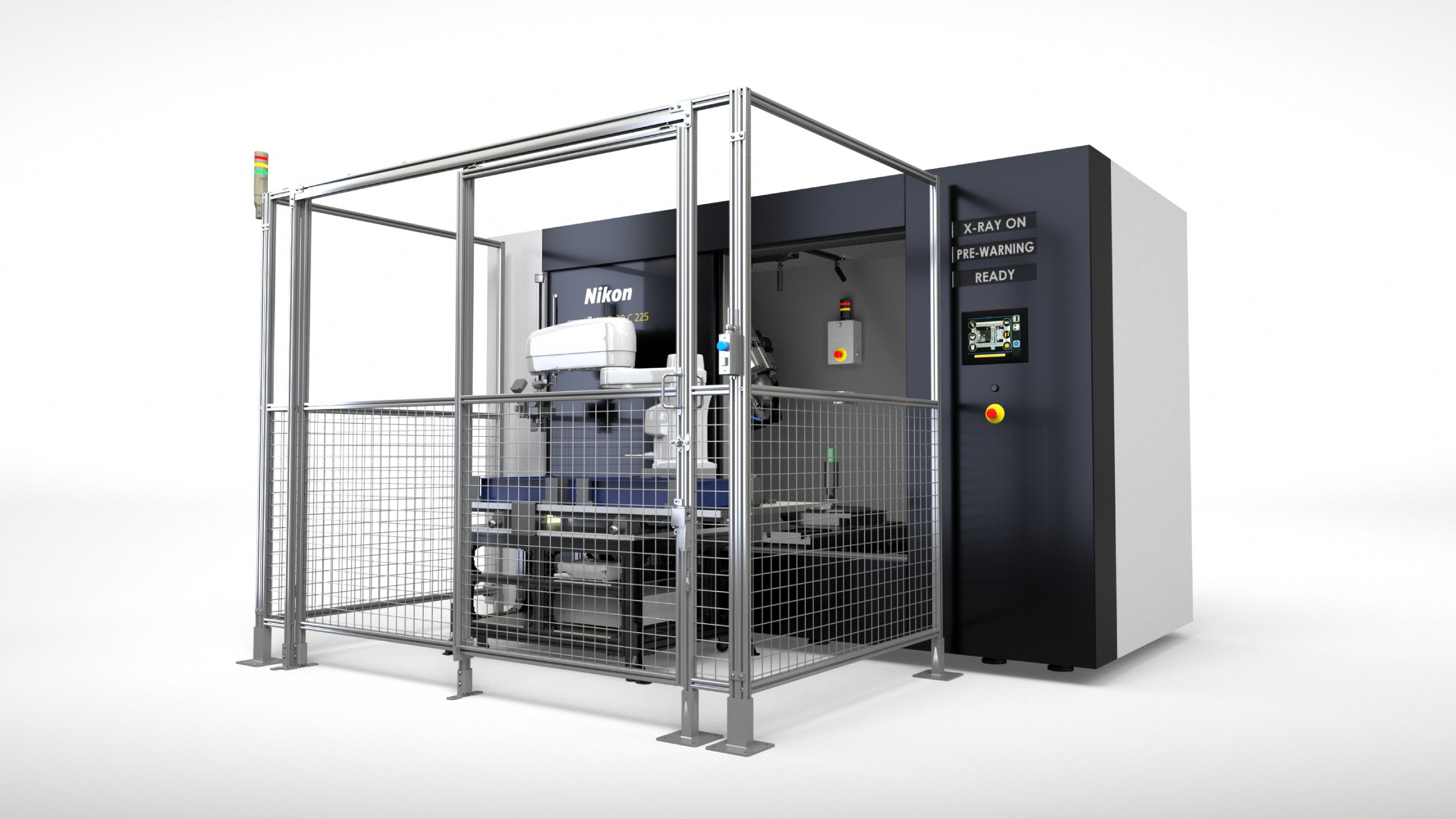
The VOXLS 30 Series enables automated, high-speed CT inspection ready for Quality 4.0 production. Robotics allow automated part loading/unloading while rapid transfer doors facilitate efficient workflows. When combined with Nikon’s Automation OPC UA Interface, the VOXLS 30 Series integrates robotic automation for repeatable, operator-independent results
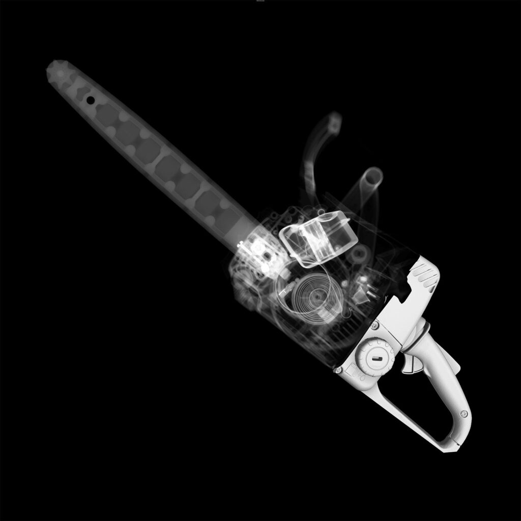
The VOXLS 30 Series delivers cutting-edge X-ray and CT scanning for production and research across a broad range of industries, providing the flexibility and image quality needed to inspect everything from intricate electronics to castings. Whether on the production line or in the lab, the VOXLS 30 Series’ automation-ready design ensures efficiency and reliability. Ideal for manufacturers in the automotive industry, aerospace, metals, medical devices, and more, the VOXLS 30 Series helps diverse industries innovate and maintain quality standards.

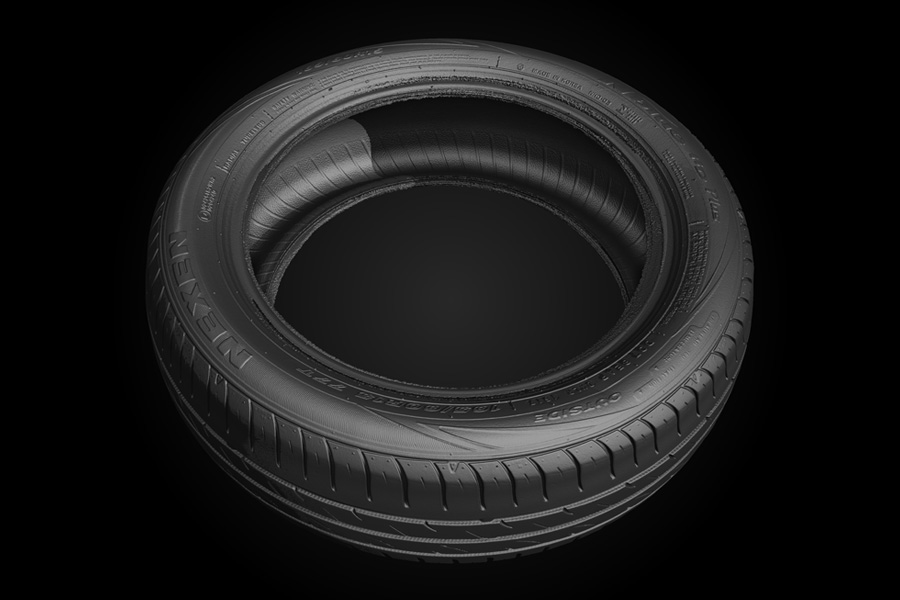
The automotive industry produces a diverse range of parts, from large engine castings to electronics. The VOXLS 30 Series provides the flexibility and penetration energy necessary to support the needs of an automobile manufacturer or supplier, whether that’s on the production line, in the R&D lab, or anywhere in between.

The rapidly innovating battery and electrification industry has growing demands, especially for improved lithium-ion performance. The VOXLS 30 Series can inspect individual cells up to fully assembled battery packs.

Efficiency and reliability are at the core of the aerospace and defence marketplace. With the correct installation, the VOXLS 30 Series enables detailed trend analysis and performance tracking following ASTM E2737 standards and produces a clear graphical visualisation of results, all within a fully automated process.
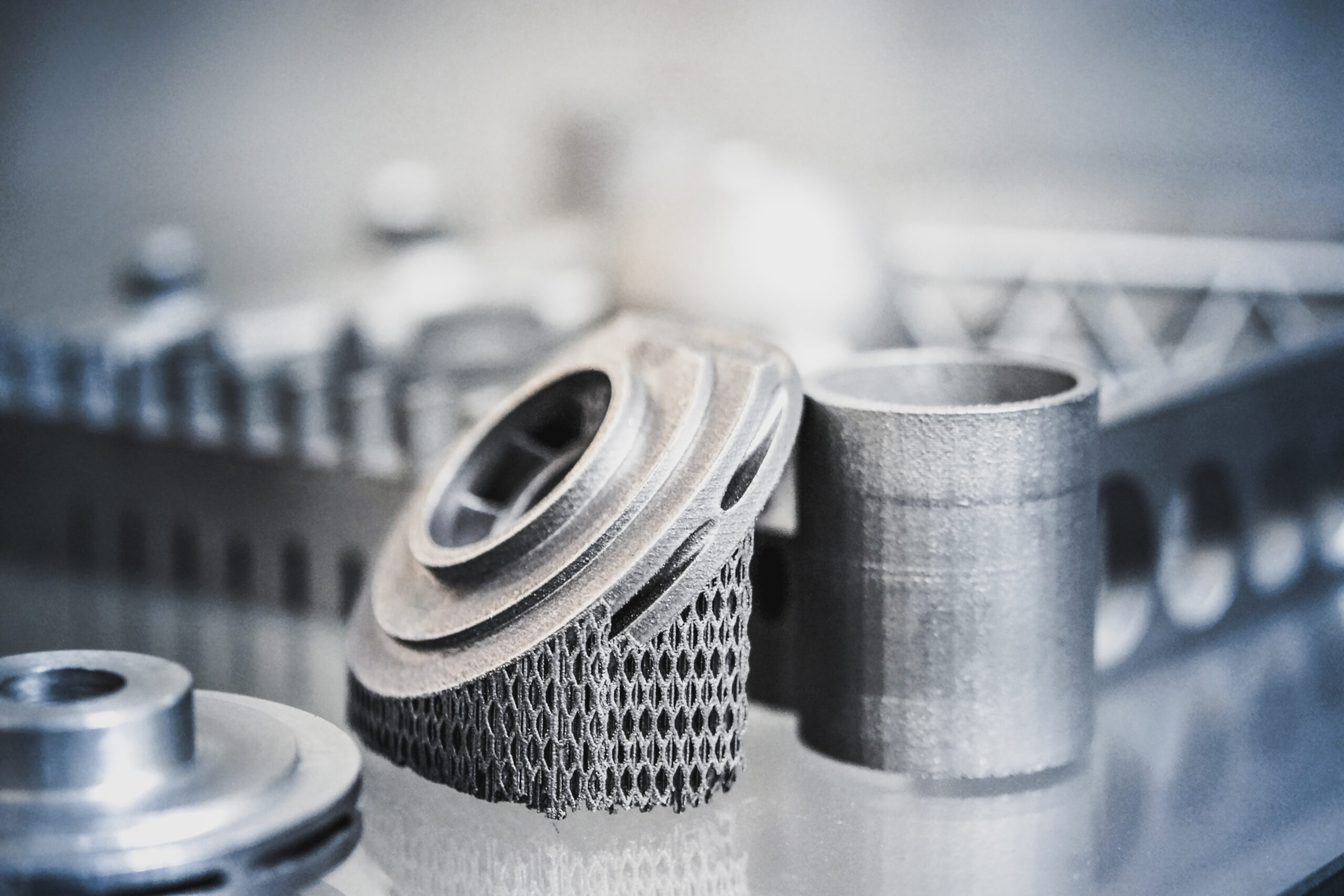
From castings to machined components and cutting-edge 3D printing, manufactured metals are the backbone of many industrial marketplaces. Whether inspecting for shrinkage on the factory floor or measuring porosity in metal additive manufactured parts, the VOXLS 30 Series has a configuration suited to meet your metal inspection needs.

Medical devices and pharmaceuticals are produced and used in some of the planet’s most demanding and highly regulated environments, with no room for failure. A faulty pacemaker or a defective surgical tool can represent the difference between life and death. The VOXLS 30 Series has the features and scan quality needed to ensure these devices function when needed.

Academic research requires some of the most diverse scanning applications of all organisations, including core samples, fossils, new blends of composites, cutting-edge alloys, plant and animal sciences, and more. The VOXLS 30 Series of systems has the scan and resolution enhancement technologies to optimise scan results and help researchers find the answers they are seeking.

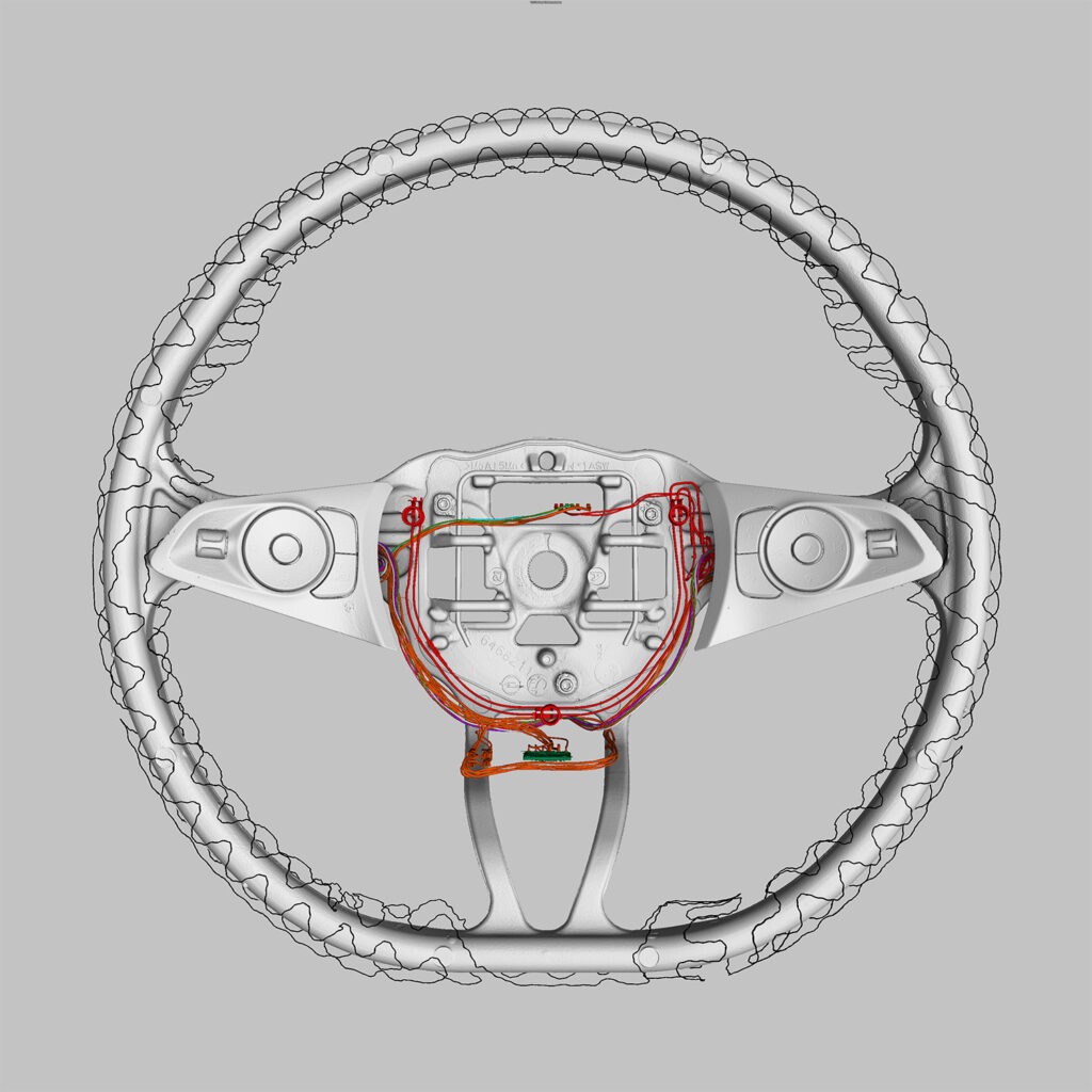
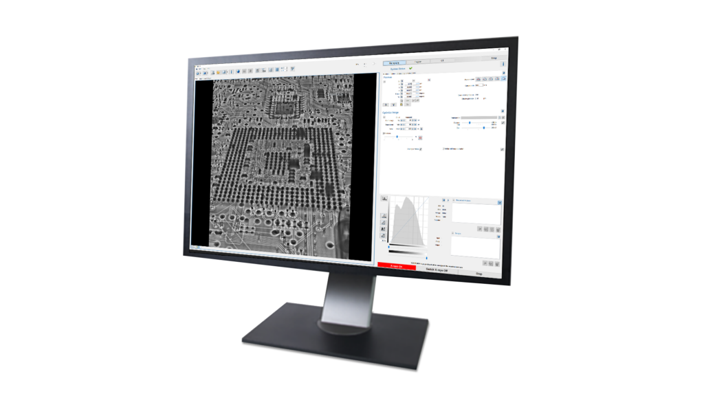
Electronics now permeate nearly everything, from microchips to multilayer circuit boards. The VOXLS 30 Series provides the resolution to detect defects in BGAs and cracks in bond wires, as well as the energy to evaluate large electronics layer-by-layer.
The VOXLS 30 Series CT systems in 225 kV, 320 kV, and 450 kV configurations optimise automated inspection with metrology-grade manipulation and proprietary sources. Providing industry-leading scan volumes, these automation-ready systems drive zero-defect manufacturing.

Your x-ray source decision will be primarily based on the size and material of your part. The larger the part, the farther the X-ray photons need to travel to penetrate and therefore, higher energy is required. Additionally, higher-density materials attenuate X-ray photons at a higher rate, and therefore, higher energy will be required to penetrate materials of higher density.
Granite is an excellent, proven platform for building precision equipment. It is extremely flat, which provides accuracy along an axis motion. It is tremendously heavy, which counters the ill effects of vibrations in a manufacturing environment. Additionally, granite is thermally stable, meaning it is highly resistant to temperature variations, ultimately contributing to greater repeatability and accuracy.
Designing a metrology grade system is a cumulation of components that all work together to contribute to a stable and repeatable platform. Ranging from the more obvious factors, such as a granite base and rigid steel manipulator towers, down to the precision encoders and ball screws, there is no single piece that defines a metrology system. It is the way all the components work together that sets a metrology grade system apart from the rest.
Focus to Imager Distance (FID) is the distance from the X-ray tube to the detector, also commonly referred to as Focal Distance. A Motorised FID is a unique feature in an X-ray system of this size and allows for the detector to move closer to or farther away from the X-ray tube. This is beneficial for technique development by allowing users to adjust geometric magnification, increase flux, and optimise the system for a wide variety of part sizes and materials.
Automated X-ray inspection is a process tailored specifically to your unique requirements. The first step is to have a detailed discussion of needs and current processes with our technical staff to determine which level of automation would be the best fit. The second step is typically benchmarking, where we scan your sample(s) to prove the feasibility of automation in your specific environment. The remaining steps can vary from simple personnel training all the way to AI learning and full production integration using Nikon’s Automation OPC UA Interface.
The system is designed for longevity by utilising serviceable components. A significant factor in this longevity is open X-ray tubes. As opposed to closed/sealed tubes, which need a full replacement if they fail, open tubes can be disassembled, maintained, repaired, and returned to service quickly. Other regular maintenance includes filament changes, O-ring changes, greasing the manipulator, alignments, and software updates. Preventative maintenance agreements from Nikon are a great way to ensure peak performance from your system.
If you would like further details on this product or a more in-depth description, our expert team will provide you with additional information and, if required, arrange an on-site visit. Talk to us in detail about your project and our experts will advise you on the best inspection system to meet your requirements. Please fill out the form opposite and we will get in touch with you shortly.