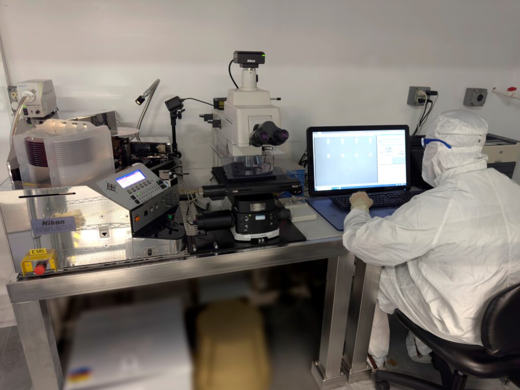
Lawrence Semiconductor has partnered with Nikon Metrology to enhance their wafer inspection processes. By integrating Nikon’s NWL 200 wafer loader system with the Eclipse L200 upright microscope, Lawrence Semiconductor has achieved higher throughput, improved accuracy, and the ability to perform 100-percent inspection of wafer lots.
Nikon Metrology has delivered a cutting-edge automated inspection solution that has revolutionized the wafer inspection processes at Lawrence Semiconductor, a leader in silicon epitaxial wafer development and production.
By integrating Nikon’s NWL 200 wafer loader system with the Eclipse L200 upright microscope, Arizona-based Lawrence Semiconductor has perfectly combined high throughput and 100-percent inspection accuracy, a previously unattainable feat.
Of all the high-tech sectors that make up advanced manufacturing, few, if any, demand the rigorous inspection protocols found in the semiconductor industry today. For these highly specialized fabs, throughput must be consistently high. Yet, that throughput is increasingly expected to be married to 100-percent inspection of the wafers used to fabricate integrated circuits. These requirements, which initially appear somewhat contradictory, are, in fact, achievable with the support of suitable metrology systems.
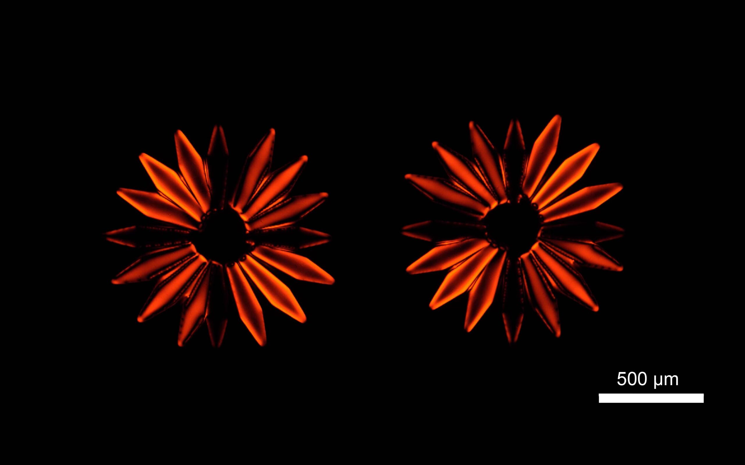
Lawrence Semiconductor, which has been in business since 1992, is a leader in silicon epitaxial wafer fabrication, providing its customers with specialized epitaxy development and production services. Epitaxy is the process of depositing highly controlled crystalline layers on silicon wafers, a critical step in the manufacturing of advanced semiconductor devices, or ‘chips.’ It’s an important process for semiconductor fabs that requires optical inspection of microscopic features on the surfaces of these wafers.
Close-tolerance inspection of large volumes of wafers requires speed and accuracy that is difficult, if possible, to achieve through manual methods. Therefore, an automated solution is needed—one that also protects these fragile wafers as they are transferred within the cleanroom from storage cassettes to inspection stations.

Automation is the key to effective inspection
Nikon Metrology’s NWL 200 wafer loader system has been designed for applications exactly like those required by Lawrence Semiconductor. Nikon’s wafer loader, integrated with the company’s Eclipse L200 upright microscope, provided a perfect solution for Lawrence Semiconductor’s unique inspection applications.
“Lawrence Semiconductor had been using our Eclipse upright microscope for inspection, but they were looking for some added solutions to automate their processes and increase efficiency and throughput,” says Cameron Davitt of Nikon Industrial Sales. “Our wafer loader, added to the microscope, accomplished these goals and made their inspection less susceptible to operator error.”
“We serve our customers with a wide range of research, development, and manufacturing capabilities, including advanced metrology and inspection,” says Ali Torabi, Chief Executive Officer of Lawrence Semiconductor. “Our partnership with Nikon is instrumental in supporting current and future inspection requirements.”
Joe Italiano, Lawrence Semiconductor’s Chief Operating Officer, agrees that the company’s relationship with Nikon has been an important part of its success.
“I joined the company 15 years ago on the process engineering side of things, and during that time, I’ve seen equipment come and go,” Italiano says. “Our metrology and inspection equipment are critical to the operation and enable us to analyze and measure our production performance. Nikon’s wafer loading system and Eclipse microscope have been strong enhancements that improved our level of service and productivity.”
Nikon’s wafer loader handles wafer diameters up to 200 mm (8-inch) and thicknesses as low as 100 µm. The wafer cassette elevator includes a non-contact centering mechanism and sensors to detect potentially distorted wafers before they are removed from the cassette. This means a smooth, safe delivery of wafers to the powerful Eclipse microscope, where various transmitted and reflected light sources help characterize their features.
“Nikon’s wafer loader and microscope give us the ability to inspect at a high resolution and in an automated fashion,” says Italiano. “It allows us to measure multiple wafers in a short period of time. We can also inspect any kind of wafer with this system, including wafers that are patterned or textured with some processing already done on them.
“Our requirement is to inspect the macro view of the surface of that 8-inch wafer under a collimated light source. We can then take it up to 500 times magnification to zero in on certain areas. You don’t want to overhandle a wafer, so this solution allows us to look at a wafer from different angles and perspectives without the need to touch or move it.”
Relying on manual transfer and measurement presents more issues than just low throughput and potential damage. Inspection quality can also be a factor.
“With patterned wafers, in the past, we’d have to analyze them manually using a bright light,” says Nick Rosson, Engineering Project Manager at Lawrence Semiconductor. “You would need to find the perfect angle to see certain defects. But with Nikon’s automated wafer loader, we can customize the rotation speed, so we won’t miss any of the key angles. Those rotational settings are really important, and the ability to flip the wafer over and inspect the reverse side is useful because, many times, the back of the wafer tells us a lot about the epitaxial growth process. All these features are very helpful.”
Throughput is name of the game
There once was a production paradigm in which customers could choose only two out of the three most critical manufacturing attributes of speed, quality, and price. Today, in highly technical environments such as semiconductor fabs, all three are required to remain competitive and achieve world-class performance. Delivering on that promise starts with maximizing throughput, with due care given to accuracy and efficiency. That, in turn, drives waste out of the system and provides the greatest possible value to the hundreds of customers who choose to work with Lawrence Semiconductor.
“Increased throughput is one of the key benefits we enjoy with Nikon’s wafer loader,” says Rosson. “For example, say we have a full cassette of 25 wafers and the customer requires 100-percent inspection. If we had to do that manually, not only would the throughput be throttled, but it also increases the possibility of unintentionally missing a defect, nicking the edge of the wafer, or damaging it in some other way. With Nikon’s automated loader, those 25 wafers can be inspected quickly and safely. Our customers are very happy because the inspections are not only fast and efficient but also of a much higher quality. We’re not going to miss any defects that might slip by during a manual inspection.”
Chris Hampton, Process Technician at Lawrence Semiconductor, explains that Nikon’s wafer loader has certain features that make it a key part of the company’s inspection processes helping to maximize throughput.
“I think the biggest improvement with Nikon’s wafer loader is that it removes operator error,” says Hampton. “Not only does it transfer the wafers from the cassette to the microscope, but it also does the complete inspection from every angle. You can pause at any angle and then send it back to the cassette. It also does the notch aligning automatically, which is very important.”
Rosson, who works closely with Hampton, underscores the importance of this feature.
“These wafers have a notch for alignment,” says Rosson. “If you performed these inspections manually, those notches won’t be aligned. We have notch aligners but using them is an extra step that the Nikon wafer loader eliminates. That helps with throughput, too.”
Because these features greatly increase throughput, the Nikon wafer loader has also helped prevent the need for sampling plans. Now, 100-percent inspection is not only feasible but expected.
“It’s all about customer satisfaction,” says Italiano. “In the past, with manual inspection, we established sampling plans where we would inspect, for example, five wafers out of 25. Now, we can consistently provide our customers with 100-percent inspection, and with Nikon’s wafer loader we fully inspect a cassette of 25 wafers faster and more accurately than we previously could inspect the five.”
Global semiconductor industry’s hyperscale future is now
The need for forward-facing inspection technologies will only grow with significant advances occurring almost daily in the semiconductor and computing space. In partnership with Nikon, Lawrence Semiconductor is well-positioned to address these rapidly emerging technologies.
“We work with many customers developing cutting-edge silicon photonics technologies,” says Mike Manago, Lawrence Semiconductor’s Chief Sales and Marketing Officer. “The end markets are cloud computing, artificial intelligence, and the hyperscale data centers being built to support these emerging applications. We also provide epitaxial services to customers engaged in quantum computing research, and develop and supply materials for power semiconductors used in commercial and defense applications. All these technologies depend on manufacturing processes with automated, 100% inspection.”
Customer requirements in hyper-competitive markets consistently drive the most significant and lasting improvements for companies striving to lead their respective fields. Lawrence Semiconductor exemplifies this reality, demonstrating how meeting stringent demands can lead to sustained excellence.
“The development and production of silicon and silicon-germanium epi wafers requires continuous investment in new capabilities, now more than ever,” says Torabi. “Lawrence Semiconductor’s partnership with Nikon Metrology provides us with the inspection capabilities needed to accomplish our mission of providing customers with innovative, cost-effective epitaxy solutions.”
“Lawrence Semiconductor has been serving the semiconductor industry for more than 30 years, and our longevity is the result of our focus on customers. With Nikon’s support, we are well positioned to enable customer success for many years to come.”
