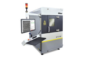
Electronics manufacturing services (EMS) companies are increasingly turning to X-ray technology to accelerate the increasingly difficult job of inspecting printed circuit boards (PCBs) and other assemblies. For example, in September 2022 MB Elettronica (www.mbelettronica-srl.it), located in Reggio nell’Emilia, northern Italy, called in the Industrial Metrology Business Unit of Nikon Corporation (www.industry.nikon.com) to install one of its XT V 160 X-ray quality control systems.
MB Elettronica’s IT manager Lorenzo Casini said,
Our main business is the subcontract production and assembly of every kind of PCB our customers outsource to us. We have to inspect the boards and the electronic components assembled onto them before delivery to ensure that they have been correctly soldered.
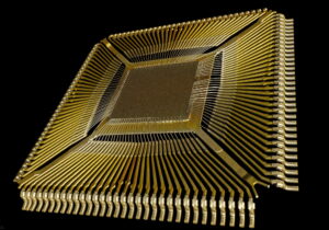
The reason we purchased the Nikon X-ray machine was so we could have full control over our production processes. It is important to keep up with the latest advances in inspection technology to be able to efficiently inspect modern component packages such as BGAs (ball grid arrays) and QFN (quad-flat no-lead) interconnections.
Their weld joints are frequently so complex and compact that it is becoming impossible to examine them with our two traditional AOI (automatic optical inspection) 3D inspection machines, so we decided that an X-ray machine was the way to go.
He explained that AOI is still used for finding a range of common problems in SMT (surface mount technology) production and soldering processes. The Nikon XT V 160 provides supplementary support for inspecting the latter in more detail and for performing failure analysis. The goal was for MB Elettronica not only to have complete control over its manufacturing, but also to make available to customers in the automotive, medical, telecoms and, in the future, even in the rail sectors a full package of reporting services.
 Several different X-ray equipment suppliers were considered at the outset. According to Mr Casini, the EMS specialist decided in favour of the Nikon solution due to its power, versatility and usability coupled with the capability of the operating software. He added, “In particular, the X.Tract laminography option and the availability of accurate report generation for every kind of inspection, such as void percentage and ball count, were a must-have for us.”
Installation of the XT V 160 was fast and trouble-free and the subsequent training was reported to be very clear for each operator involved. The X-ray capability is already being used for sample inspection to support production batch validation and to optimise soldering parameters. It now forms part of every PCB manufacturing process at the Reggio nell’Emilia factory.
Mr Casini concluded,
Previously, when inspecting some bought-in products by AOI, we could not see any voids on the weld joints of the components, but they nevertheless failed the functional test. Thanks to the Nikon X-ray machine, we were able to find that there were some voids within the components and so find the cause of the test failures.
In the long run, with our X-ray testing and failure analysis able to support our production process control, we expect to increase the number of customers that come to us and to retain our existing customers more easily.
About the Nikon XT V 160
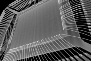
The X-ray machine provides a generous 406 mm x 406 mm maximum scan area, large enough for most PCBs, and its comprehensive specification includes Inspect-X control, analysis and reporting software written in-house by Nikon engineers. The equipment has variable magnification, a tilting flat panel detector and a powerful, 160 kV / 20W X-ray microfocus source, which generates a spot size down to 1 µm for incredibly high resolution.
A board can be viewed at oblique angles of up to 72 degrees, enabling clear sight of solder joints and through-holes while maintaining sufficient X-ray energy. The output is exceptionally stable to prevent noise degrading the image that is captured and processed. This is essential if potential defects are to be identified in next-generation interconnects and packaging technology.
When inspecting BGA solder joints, an operator needs to gain a clear view of each ball interconnect, which is traditionally achieved by manipulating tilt and rotate movements while scanning down the rows. The XT V 160 enables this function using single-axis control, so the operator can concentrate on the inspection rather than on guiding the machine.
True concentric imaging makes it easy to lock onto the area of interest and rotate the view point through 360 degrees. Once a region on a PCB has been identified and positioned in the centre of the screen, it remains fixed there no matter what tilt, rotation or magnification is applied.
Included in the turnkey package supplied by Nikon to MB Elettronica was optional X.Tract laminography. The automated acquisition capability uses the manufacturer’s advanced CT (computed tomography) reconstruction algorithm to generate virtual 3D micro-sections of a sample in any orientation.
The hardware and software combination provides clear images coupled with seamless transition between 2D radiography and 3D laminography in one system. The user therefore gains better insight into the presence of faults such as voids, cracks and misalignments in complex electronics.


