REM Surface Engineering turned to Nikon and its high-resolution X-ray technologies to discover internal defects and surface roughness in parts that other methods couldn’t detect, helping solve a key problem for its industry customers.
X-ray computed tomography (CT) technology provided by Nikon has enabled REM Surface Engineering to transform their unique – and highly challenging – test and inspection applications. Operating at the cutting edge of engineering excellence, Connecticut-based REM Surface Engineering has gained a crucial advantage through its partnership with Nikon and its high-resolution X-ray CT scanning systems. These advanced imaging solutions have empowered REM Surface Engineering to uncover internal defects and surface irregularities in their clients’ components that were previously undetectable by conventional methods.
Founded in 1965, REM Surface Engineering has established a patented isotropic superfinishing technology for metallic components. A wide range of alloys can be finished by REM Surface Engineering, including parts that are manufactured through either traditional subtractive or more recently developed additive processes. Sectors such as space, aerospace, automotive, and defence require components with optimised surface textures to meet their applications’ specific performance requirements including increases to contact fatigue and bending fatigue resistance, improved flow to reduce turbulence and pressure drop, and many others.
“We have a pure chemical polishing technology,” says Justin Michaud, President and CEO of REM Surface Engineering. “It’s like a more refined version of chemical milling or chemical etching, where we’re far more precise in our application of these products, both from a formulation perspective and across the application perspective, to be able to control how we’re altering that surface texture. Additionally, we have a combinatory chemical-mechanical polishing process that utilises alloy-matched chemistries to enable gentle surface refinement via specialised mass-finishing approaches; this technique is able to maintain component geometries to a much higher degree than traditional, abrasive processes, and it can further reduce surface texture as necessary.”
That alteration of surface textures creates a degree of smoothness crucial to REM Surface Engineering’s high-tech customers, whose final products often demand the greatest possible reduction of surface roughness and deformities, however minor they may appear.
“Gears, airfoils, rocket engines, and other precision components benefit from smoother surfaces in terms of contact fatigue, airflow efficiency, or dealing with harsh operating conditions,” says Michaud.
Validation through Nikon X-ray Micro CT Scanning
Many of the parts that go into completed assemblies are currently created through additive manufacturing, which initially created some bottlenecks for the REM Surface Engineering team.
“Almost 15 years ago, the aerospace manufacturers that we were working with became some of the first companies to jump into the metal additive manufacturing space in a meaningful sense,” says Michaud. “When those parts began to arrive, they obviously looked very different than the precision, machined or milled components that we were used to.”
Flaws like porosity, pitting, and waviness can all substantially and negatively affect the performance of component assemblies. Being able to identify these issues without destroying the parts – and then proving to the customers how the REM Surface Engineering process positively affected the smoothness of those surfaces – is crucial to the company’s continued success.
Michaud explains the surface characteristics of additive manufactured parts are quite different from those produced by more traditional manufacturing processes.
“These are more complex than machined surfaces,” agrees Agustin Diaz, Ph.D., REM Surface Engineering’s Advanced Manufacturing and Innovation Manager. “The additively manufactured parts have really rich types of surface textures.”
As samples of these parts came in from customers for testing and analysis, it became clear that there were some questions about the near-surface integrity, specifically regarding porosity.
“Ours is a chemical finishing process, so we’re always looking to make sure that we’re not causing intergranular oxidation or pitting,” says Dr. Diaz. “Mid-process, as we were reducing the surface texture, we were beginning to see some weird stuff emerge.
“I thought that perhaps we were pitting the sample through our process, but it turned out that the problem was the samples themselves, which had all these internal defects that we could not see or characterise until we either did a destructive analysis or a high-resolution X-ray CT scan.”
Revealing the truth with Nikon X-ray CT
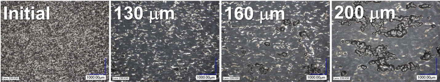
The phrase “high-resolution” is key here, because, in some cases, the customers may have performed their own X-ray CT analysis on the parts, which showed no porosity.
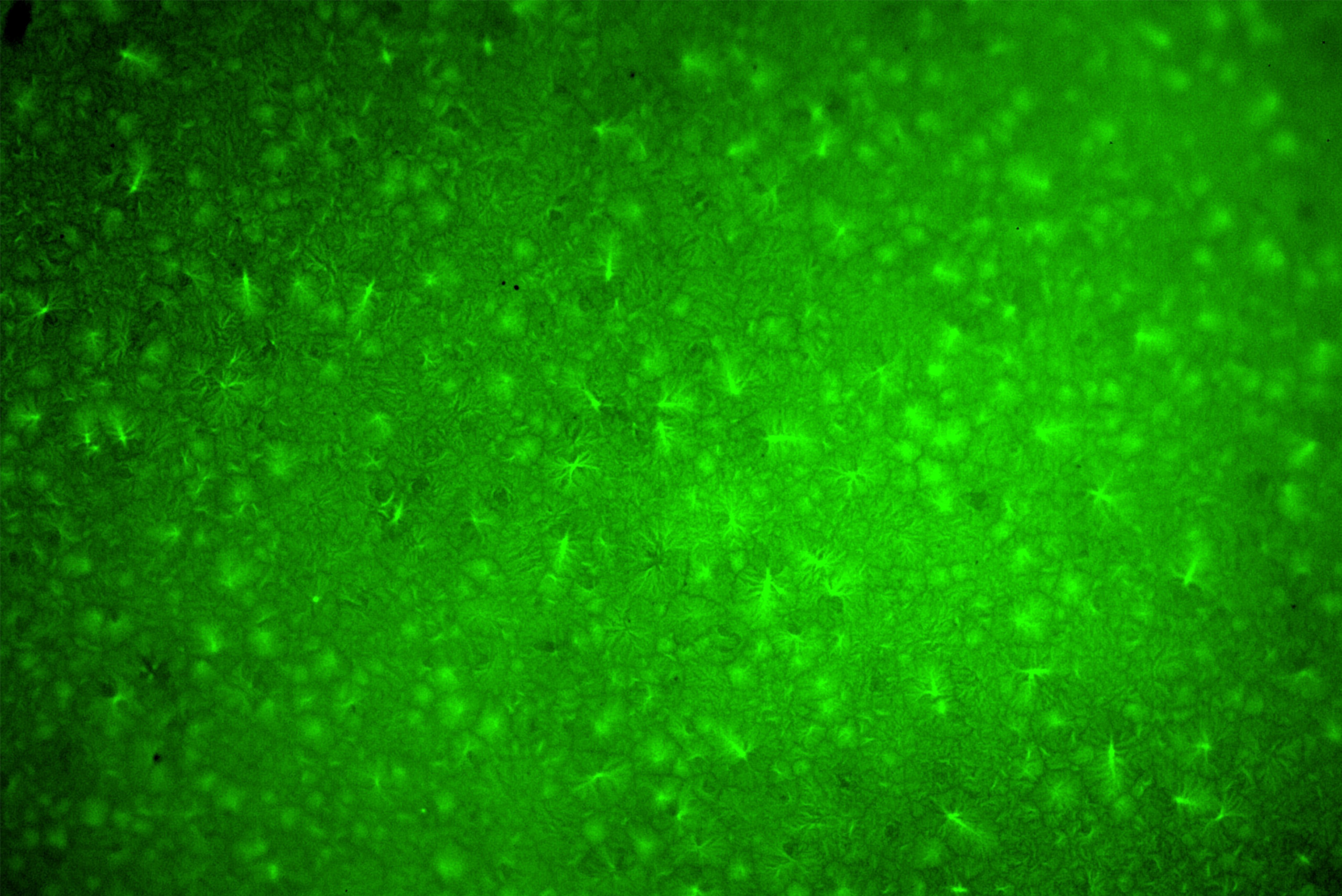
“I would ask them what voxel size they used for that inspection,” explains Dr. Diaz. “Most times, it would be around 90 microns. Well, you’re not going to see the level of detail necessary at that resolution. They may believe they had no porosity, but when you start processing the part and remove 50 or 130 microns from the surface, you see how the surface evolves and can observe all these ‘hidden’ flaws popping out.”
“When you have the higher-resolution X-ray CT scan, you can see all the porosity accumulated in the near surface of the sample. So, this part that was supposed to be 100-percent dense is not that dense – and the porosity is also highly anisotropic.”
This highlights the advantages of Nikon’s high-resolution X-ray CT scanning capabilities, according to Brian Barlow, National Business Development Manager of Nikon’s X-ray CT Inspection Services.
“Our rotating target microfocus CT technology allows us to achieve some of the highest resolution scans in the industry, particularly on higher density samples,” says Barlow. “These high-quality scan results have been crucial to the success of our projects together with REM Surface Engineering.
“Many of REM Surface Engineering’s customers need to see the initial condition of the part versus the post-processing finish that REM provides,” Barlow continues. “Nikon X-ray CT Inspection Services scans both the initial processed part and post-processed finished surface and allows the accurate measurement of those differences – and we do it nondestructively.”
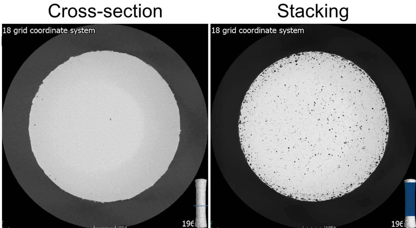
The partnership with Nikon allows REM Surface Engineering to demonstrate the value of its process. Parts that appear smooth to the naked eye and even pass initial X-ray scanning are shown to have defects when examined by Nikon’s advanced X-ray system. After chemical polishing, rescanning reveals a dramatic improvement in surface smoothness, which leads to significantly better performance for the final products. The ability to prove these tangible benefits is why customers keep coming back to REM Surface Engineering.
Talking the same language
The partnership between REM Surface Engineering and Nikon Metrology is successful because both companies have a strong foundation in engineering principles and scientific fundamentals. Their teams speak the same language and can effectively collaborate to develop innovative solutions together.
“The Nikon team has been really helpful in dealing with a wide range of alloys,” says Michaud. “We’ve come to them with aluminium components, titanium components, nickel superalloy components, and copper components. Those materials scan differently, but together, our teams have been able to support all those needs and applications.”
Dr. Diaz agrees that the strong level of support offered by the Nikon team when it comes to REM Surface Engineering’s specific requirements has been an important part of the successful collaboration.
“They’re always there to help you with the technical questions that you have right in the middle of a project,” says Dr. Diaz. “If we get stuck on some specific element of a scan, we just call, and five minutes later, we have an answer – plus a beautiful picture to put in a report or to show the customer. That level of customer service is great.”
As manufacturing applications become more complex and measuring surface finishes gets more challenging, the engineers at REM Surface Engineering and Nikon will enhance their processes to provide better surface finishes that meet the increasing demands across various industries.
And as advanced manufacturing techniques like 3D printing become more widespread, ensuring smooth surface finishes on parts will be critical. Nikon’s precise X-ray CT scanning systems allow companies to inspect and measure surface characteristics without destroying the part. This nondestructive, micro-computed tomography testing capability is an essential part of the manufacturing workflow. It enables a cycle of continuous improvement, where surface finishes get better and better, providing increasing benefits.
“We’ve been so happy with the Nikon team,” says Michaud. “They’re responsive, reasonably priced, and great at what they do. That’s why we’ve been so loyal. We wouldn’t even consider any other option.”


