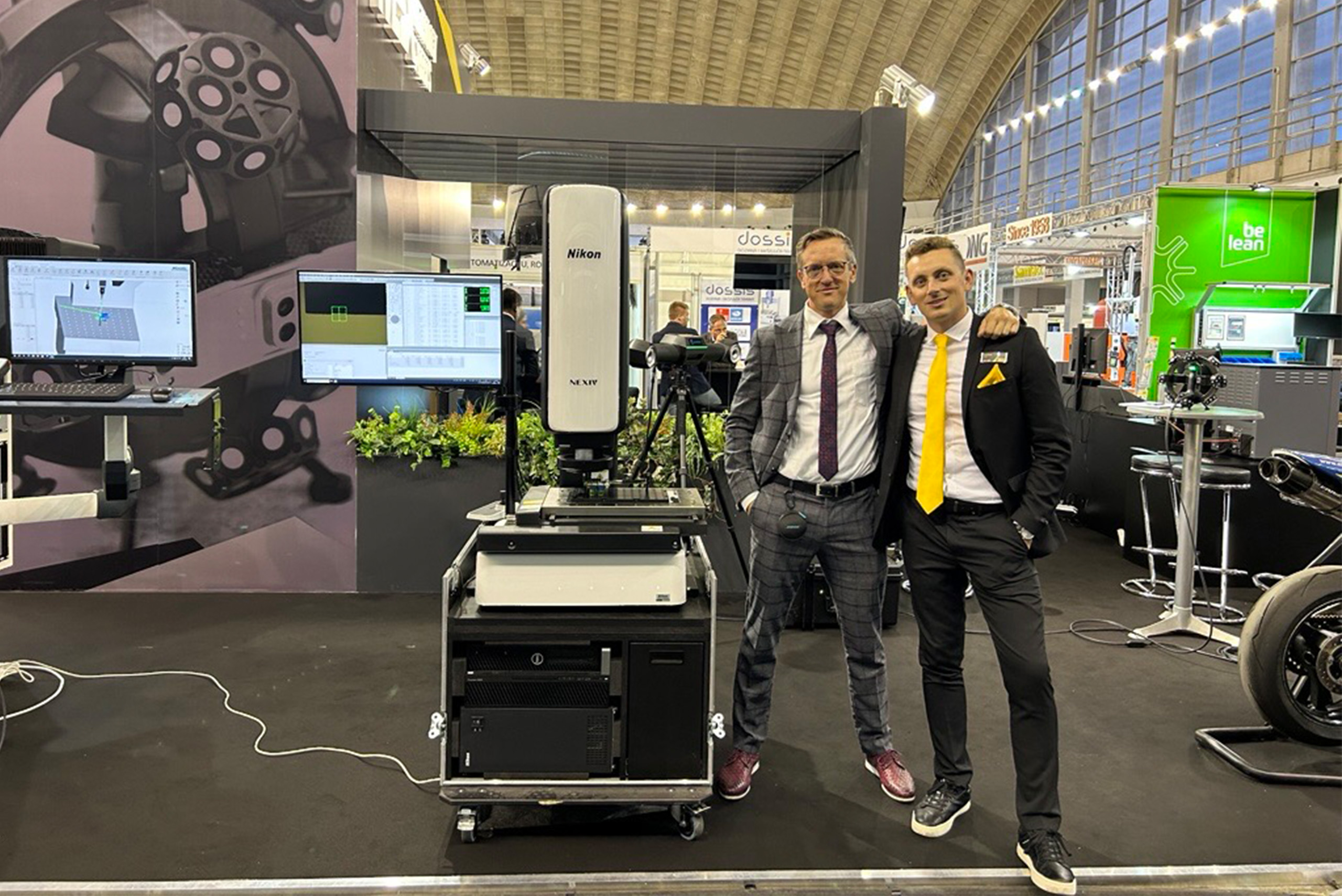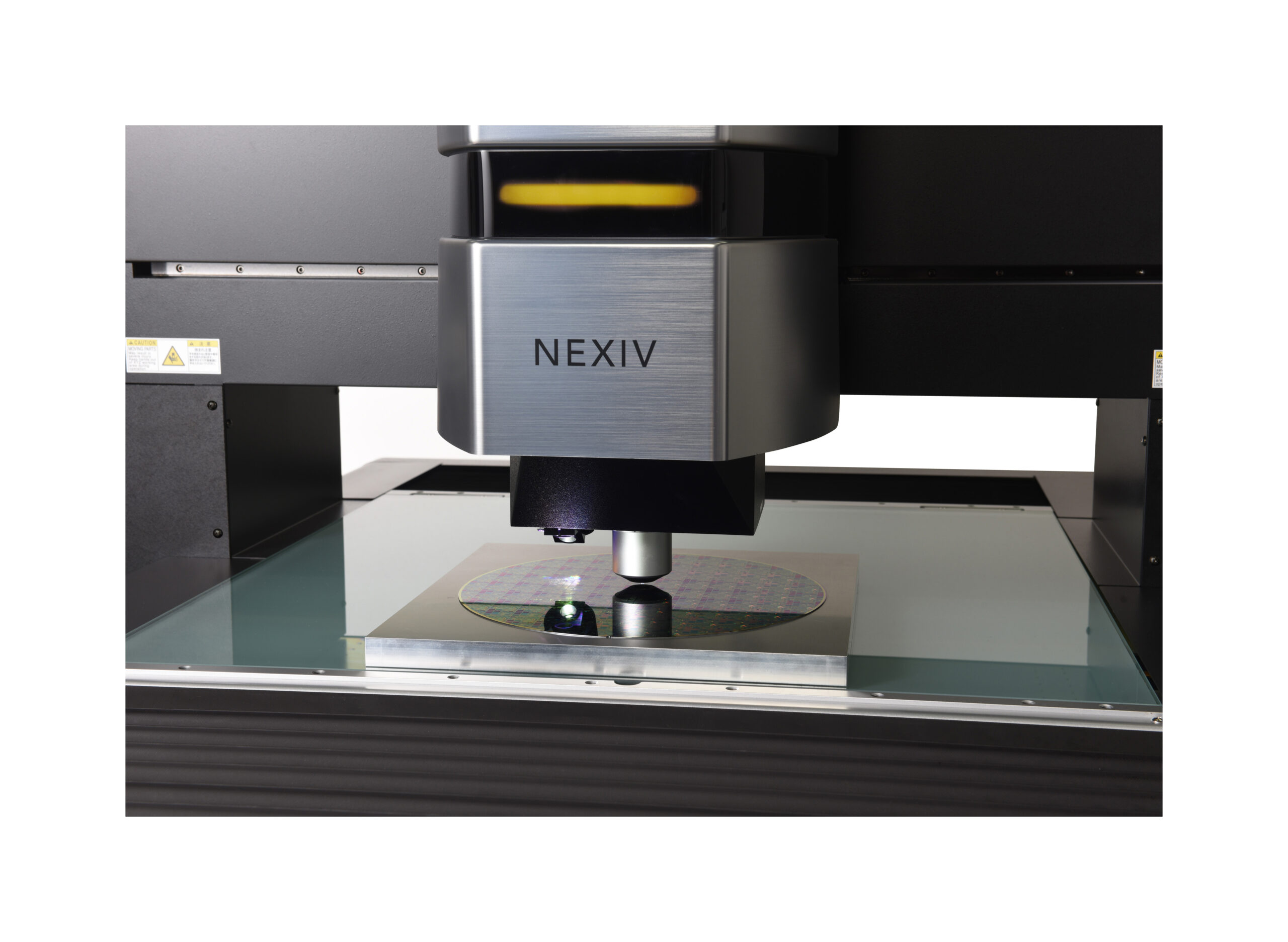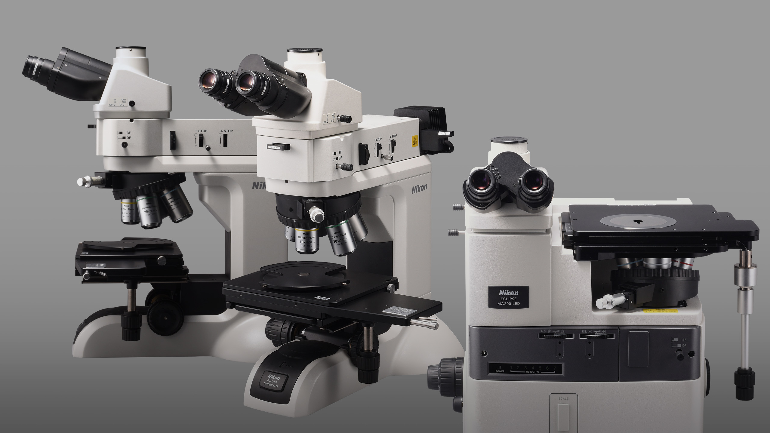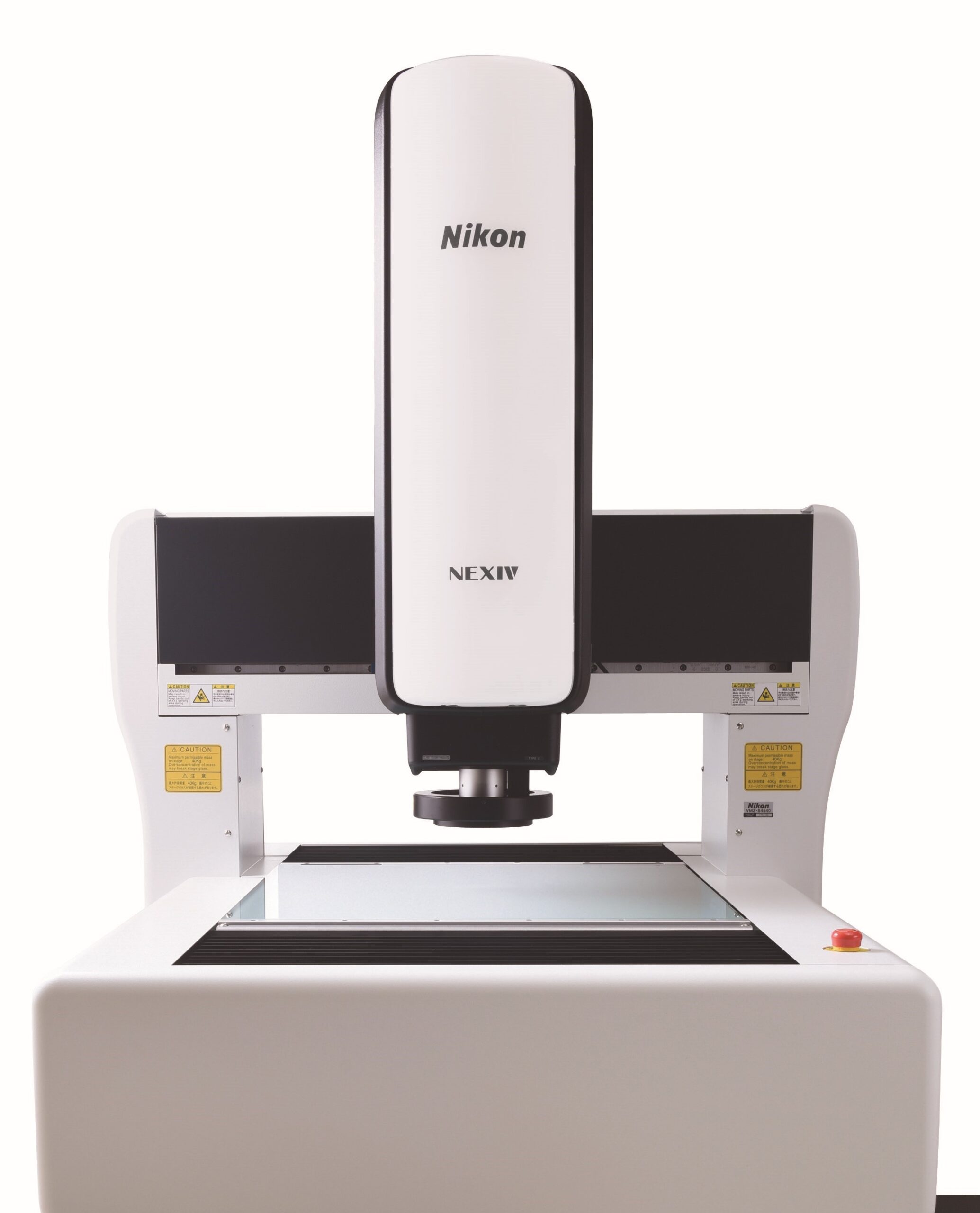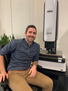
We spoke to our NEXIV Application Engineer, Philipp Wachenfeld – who has worked vastly on semiconductor projects with fully automated metrology tools, about his knowledge and experience with wafer inspection using the NEXIV’s.
Hi Philipp, please can you talk us through Wafer Inspection in the Semiconductor industry & the different requirements the Nikon NEXIV can accommodate?
Of course! The Semiconductor industry is a fast growing and developing industry with a very high level of requirements that need to be fulfilled by the suppliers. This applies to the optical metrology systems that are indispensable in all kind of stages during the processing of wafers – starting from the first bare wafers to fully developed and isolated chips.
Nikon is working with suppliers for the wafer handling systems that have years of experience in the semiconductor industry. In many clean room fabs of the semiconductor companies, the operator influence is reduced to a minimum. That’s why we offer our NEXIV systems with fully automated handling units, that are adapted to the customer demands. The combination of the NEXIV tool and the automated wafer handling units are extremely well suited for companies striving for Industry 4.0.
We at Nikon can provide handling tools for all kinds of wafer sizes and shapes and install load ports for the requested wafer cassettes. Our tools can be equipped with up to 4 load ports, depending on the wafer sizes and the exact tool configuration. The same works with the end effectors: depending on the customer requirements and wafer types, our suppliers can offer a solution.
The full automated circle of Wafer inspection with a Nikon NEXIV will look like the following:
- The operator places a cassette/FOUP with wafers on a load port on the metrology tool
- The robot unit scans the cassette/FOUP to register how many wafers are loaded in the cassette
- The robot unit then picks up one wafer from the cassette/FOUP and places it on a pre-aligner
- The pre-aligner corrects the wafer rotation and position
- (The Wafer-ID or a barcode on the wafer can be read additionally using a scanner next to the pre-aligner)
- The robot unit takes the wafer from the pre-aligner and places it on the measurement stage
- Measurement is then performed using our NEXIV system
- After the measurement is complete, the wafer will be transferred back to the cassette
As simple as it sounds, there are a lot of variations at every step that might complicate the overall system, which is why myself and our NEXIV team are on hand to ensure our customers bespoke requirements are met.
Samples/Wafers:
Bare wafers usually consist of silicon, but can also be made out of glass, silicon carbide, germanium, gallium arsenide and other semiconductor materials. Wafers are processed in sizes between 2” and 12” (2”, 4”, 6”, 8”, 12”) and run through various process steps until the product is finished. Most critical aspect for the handling of the wafer is the thickness of the wafers and the warpage, meaning how strongly the wafer can bend. The thickness varies from ~0.1 mm up to a few mm and the warpage from few micrometres up to a few millimetres.
In some process steps in wafer manufacturing, it is necessary to protect the wafer surface. This is completed by applying tape on the wafer or even place the wafer on the tape in a frame (often used for wafer grinding or dicing applications).
A wafer load port is where the operator in the clean room will place the cassette/FOUP with the wafers inside which need to be measured – the load port can automatically detect what kind of cassette/FOUP is placed in the machine. Wafer sizes and number of slots of the cassettes are then detected by the system. Single load ports can also be used for different wafer sizes (e.g. 6” and 8” wafers, which is a quite common combination).
End effectors:
End effectors are the part of the robot handling unit which actually grabs the wafer to complete the inspection. Depending on the size, thickness and shape of the wafer the right end effector has to be selected. There is a wide range of possible handling ways, from simple vacuum end effectors, over needle end effectors, to so called edge-grip end effectors that only barely touch the sensitive wafer surfaces. Fully automated tools can also be equipped with an end effector changing station, so the customer can simply handle different types of wafer sizes and shapes.
The end effector is part of the robot arm, NEXIV’s can be equipped with one robot arm but also with a dual arm robot to increase the throughput of the machine. There is also an option to place the end effectors on one robot, to handle different wafer sizes or wafer types with the same robot.
Prealigner:
The pre aligner corrects the wafer orientation on the system. It will correct the rotation the wafer may have coming out of the cassette/FOUP and the position. The end effector helps the robot to place the wafers exactly in the same position on the measurement stage, so the measurement system only needs to adjust the measurement position slightly.
Additionally, a scanner can be installed next to the pre aligner to scan the wafer ID or a barcode embedded on the wafer. This will help to identify the wafer and automatically link the measurement results to the correct wafer.
Flipping station:
In some rare cases there might be the need for the customer to flip the wafer to actually measure on both sides. This can also be completed in the wafer handling, it can either be implemented by having a robot and end effector that uses vacuum to grab and flip the wafer over or by an additional wafer flipping station, where the wafer is placed and then flipped.
Chucks:
For the measurements on the NEXIV stage, the wafer is placed on customised wafer ‘chucks’. These chucks are mounted on the stage of the NEXIV in a way that is easily accessible by the robot handling. These chucks might use the vacuum to flatten and hold the wafer on the stage or only carry the wafer on 3 points on the wafer edge. It depends on how much contact the wafer is allowed to have and if a diascopic illumination for the measurement is needed.
If you have found the information which Philipp has provided a great insight and would like to learn more about Wafer Inspection using a Nikon NEXIV, please contact our team to find our more about Nikon NEXIV series:
