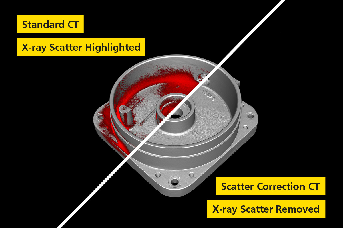
Nikon has announced the launch of Scatter Correction CT, a software solution that enhances image quality and measurement accuracy in industrial computed tomography (CT) scanning by correcting scatter artifacts.
Leuven, Belgium – Nikon Metrology NV (Nikon Metrology), a subsidiary of Nikon Corporation (Nikon), has announced the launch of Scatter Correction CT, a software solution designed to address the challenges posed by X-ray scatter artifacts in industrial computed tomography (CT) scanning. By employing advanced physics-based modelling techniques, Scatter Correction CT significantly improves image clarity and measurement accuracy, particularly for dense materials such as aluminium, steel, ceramic, and Inconel.
X-ray scatter artifacts have long been a significant issue for CT scan operators, hindering their ability to obtain clear images of internal and external structures. X-rays, like visible light, typically travel in straight lines but are sometimes absorbed and re-emitted, which can change the direction of travel. This issue can manifest as cloudy haloes surrounding high-density regions, false inhomogeneities within homogeneous regions, and edge blurring across material boundaries. Scatter Correction CT effectively simulates and corrects for these complex interactions, removing the detrimental effects of scatter.
Key benefits of Scatter Correction CT include:
- Enhanced image clarity: By correcting for X-ray scatter artifacts, Scatter Correction CT dramatically improves image quality, enabling more precise visualisation of internal and external structures, defects, and fine details.
- Improved measurement accuracy: More precise and reliable measurements of component geometries and internal features, critical for quality control and Industry 4.0 manufacturing.
- Significantly faster scan times: More than 100 times faster than traditional scatter-free 2D CT methods, allowing manufacturers to significantly improve throughput and accelerate product development.
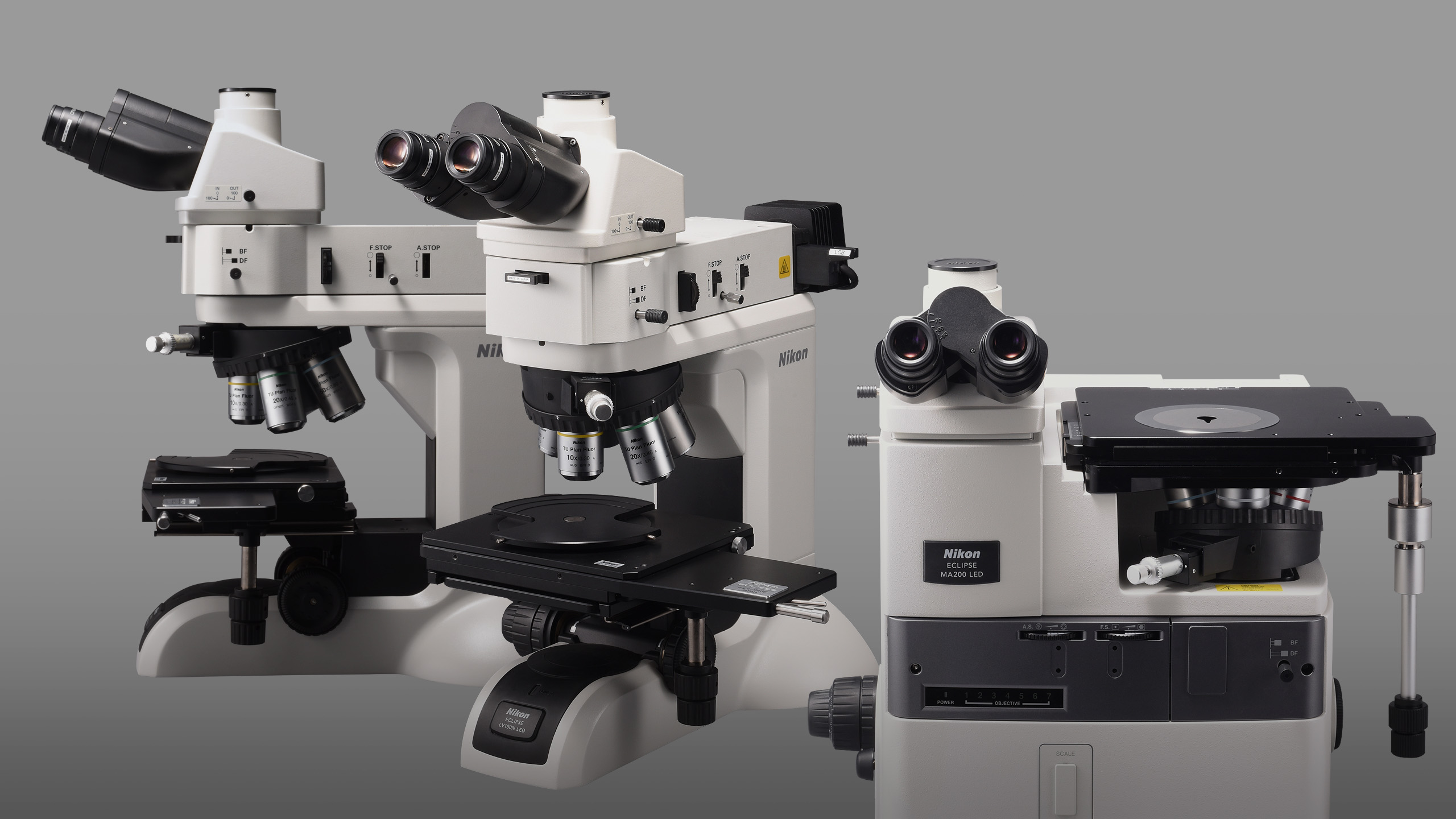
- Wide compatibility: Scatter Correction CT is available across all Nikon X-ray sources and systems in the 225 kV and above range and is fully compatible with all Nikon CT scanning acquisition modes, providing a versatile solution for diverse industrial applications.
- Ease of use: The correction is seamlessly integrated into the scanning workflow, requiring only a single click to enable. This reduces the need for specialised skills and improves overall productivity.
Scatter Correction CT substantially benefits various industries, including aerospace, automotive, additive manufacturing, and castings.
“We are excited to introduce Scatter Correction CT, a game-changing solution that addresses a critical challenge in industrial CT scanning,” said Nikon’s X-ray and CT Global Product Manager Dr. Andrew Mathers. “By correcting for X-ray scatter artifacts, our software provides manufacturers with significantly better image quality and measurement accuracy in their CT scans, ultimately enhancing quality control, product development, and research capabilities.”
Nikon is actively reaching out to existing customers to showcase the advantages of Scatter Correction CT. New customers are encouraged to contact their local Nikon representative to arrange a demonstration and discuss how this innovative software can benefit their specific applications.
About Nikon’s IDSBU
Nikon’s Industrial Solutions Business Unit (IDSBU) is a cornerstone of the company’s B2B operations, formed through the strategic merger of the Digital Solutions Business Unit and Industrial Metrology Business Unit. The IDSBU delivers comprehensive industrial solutions ranging from high-quality optical components to sophisticated measurement and inspection systems. The unit draws on over 100 years of Nikon’s advanced applied optics and precision technology expertise to deliver innovative solutions worldwide. Editor’s note: IDSBU is the official abbreviation for Industrial Solutions Business Unit, based on the English translation of the division name. www.industry.nikon.com
On behalf of:
Nikon Metrology Europe EV
Interleuvenlaan 86, B-3001 Leuven, Belgium.
Contact: Mona Noujeim, X-ray Marketing Manager Europe
Tel: +32 16 74 01 01
Email: [email protected]
Web: www.industry.nikon.com
Distribution:
4marcom + PR!
Siedlerstraße 33
D-85716 Unterschleißheim
Tél : +49-89-37002940
Contact : Theo Drechsel
Email : [email protected]
Web : www.4marcompr.de