Headquartered in Cambridge, UK and with a production facility 200 miles north in Sedgefield, PragmatIC Semiconductor (www.pragmaticsemi.com) is a world leader in the manufacture of ultra-low cost, flexible electronic devices. Its embedded FlexICs (flexible integrated circuits) allow industry-wide designers and innovators across the world to create remarkably novel solutions that are not practical or even possible using traditional silicon materials.
The company also offers standard FlexIC products capable of extending proven applications such as RFID and NFC, with the potential to enable trillions of smart products and consumer goods to interact with consumers and their changeable environments as well.
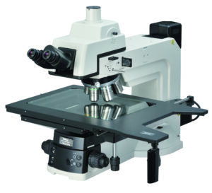
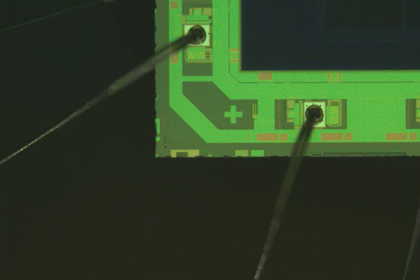
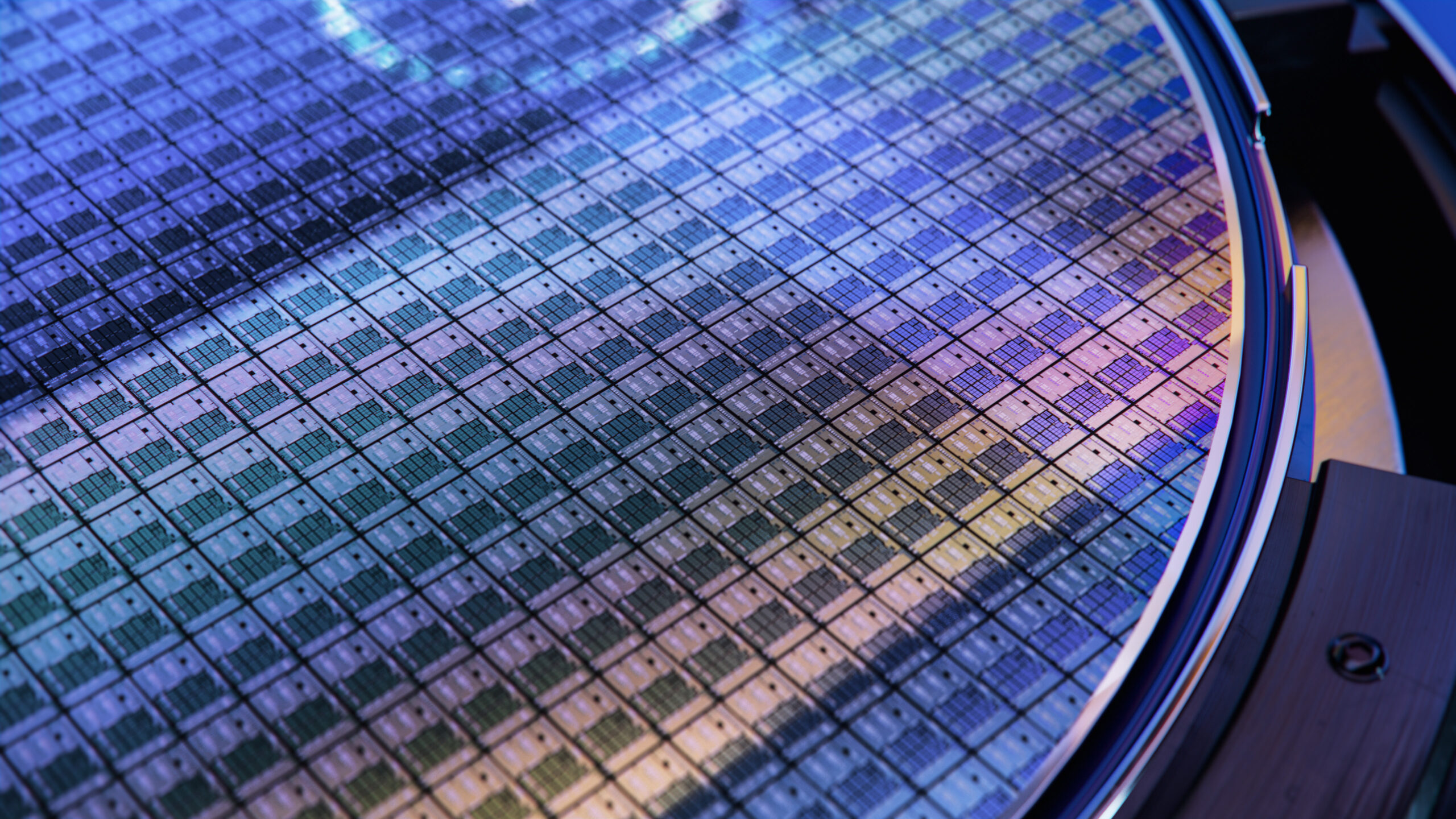
Thinner than a human hair, these ICs challenge the company’s QA processes in the metrology department during the multiple, rigorous inspection and measurement procedures; many of which are now carried out using a Nikon Eclipse L300ND trinocular optical microscope, fitted with a superb Digital Sight camera from Nikon Metrology
PragmatIC’s laser process development engineer William Harrison explained: “Throughout the processing of our integrated circuits, we require detailed inspection so we can detect any damage or imperfections and be confident we are sending the best products to our customers.
“Until recently, we used a microscope in our laboratory that had relatively low magnification and was equipped with a camera whose resolution was also limited.
“It was difficult to achieve good quality when viewing specimens at high magnifications and camera images were often blurry and unclear.
“Furthermore, the PC camera software ran slowly and movement of the stage was not smooth. All these issues increased inspection time.
“We needed a high magnification scope to aid in our detailed inspections of sometimes very small features using episcopic or diascopic functionality, and we also required the ability to capture high-quality images.”
Regarding the company’s decision to invest in the Eclipse L300ND microscope, William explained that both he and a colleague had previously praised Nikon Metrology’s microscopes’ ease of use, and the ability to capture high quality images – once major drawbacks of the previous inspection equipment. Additionally, Nikon’s universal software suite platform NIS-Elements contains features that optimise the full inspection process, from image capture to enabling a variety of processing steps, measurements and concluding quality reports.
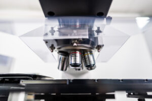
The primary target industries for the Eclipse L300ND are Semiconductor electronics and telecommunications, as well as for inspection of flat panel displays, large-scale integration electronic devices and antennae waveguides. Nikon Metrology’s CFI60 and CFI60-2 optical objectives are incorporated for flawless inspection and image recording. Combining this with advanced illumination and optical contrast systems, for diascopic as well as episcopic, brightfield, darkfield, simple polarising and differential interference contrast (DIC) microscopy techniques, produce images of high contrast and resolution. The NIS-Elements software suite efficiently manages the Nikon Digital Sight camera, capturing optimal images as well as organising and processing them logically in a smooth workflow together with the relevant test data and conclusions.
Mr Harrison concluded:
Installation of the microscope did not take long and the training provided by Nikon Metrology was easy to follow and understand. I have been very happy with the information and support given.
Taking images and measurements is much faster now, so inspection time per wafer has certainly been reduced. Using the DIC microscopy attachment has added an unexpected benefit by helping us to find defects in specimens that have little brightfield contrast.


