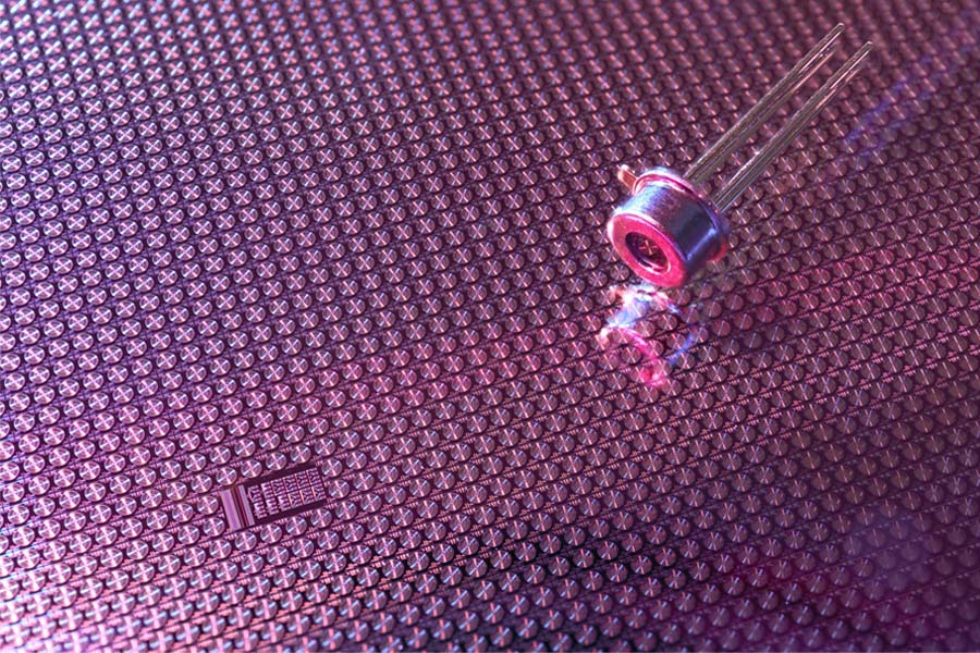
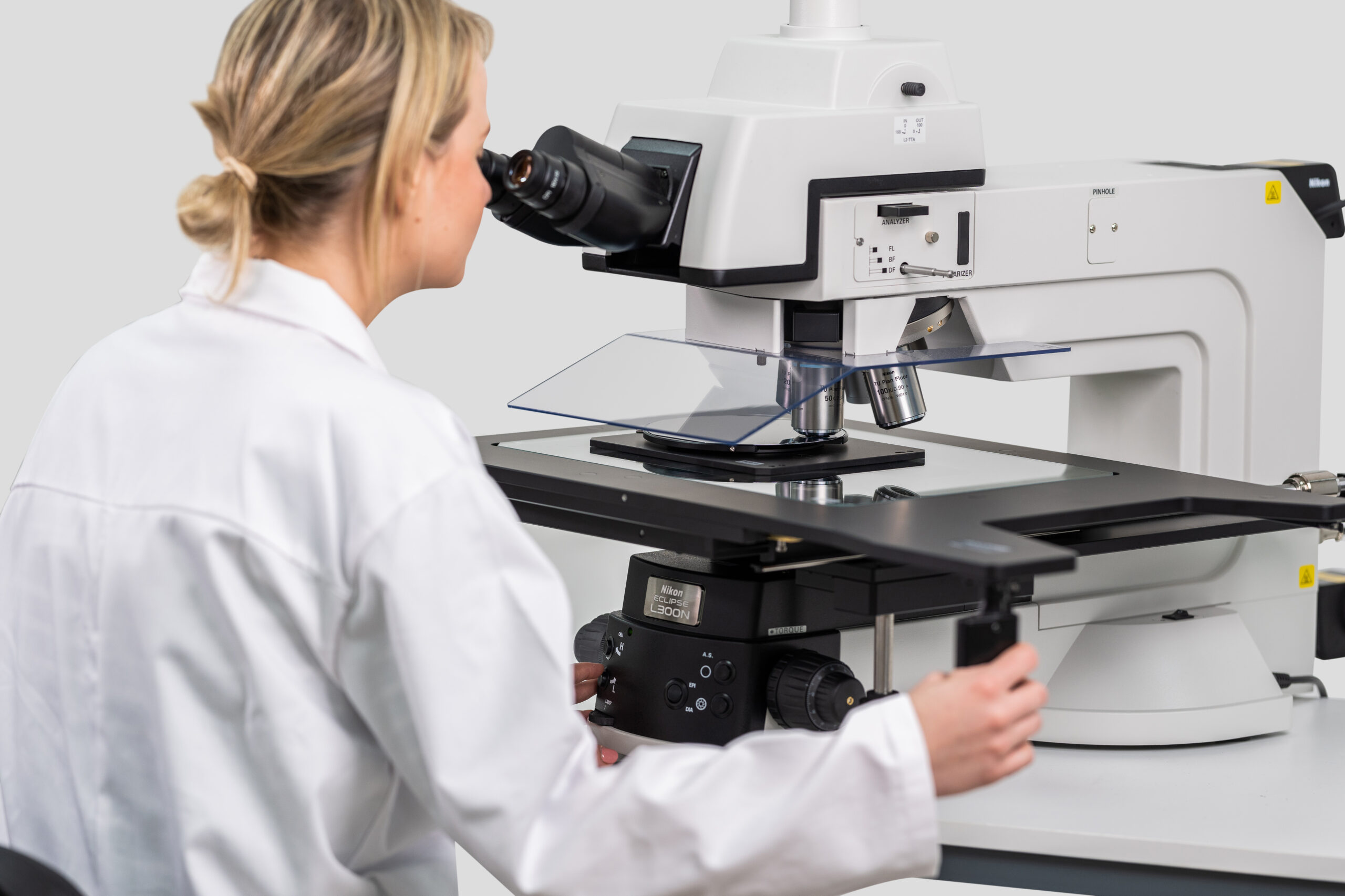
Lead frame is the most cost-effective interconnect technology for the fabrication of integrated circuits (ICs) and other electronic devices, and is used in the assembly of the vast majority of semiconductor packages. Inspection of such circuits has traditionally involved a measuring microscope or machine that is manually operated.
However component handling is slow, and metrology throughput is limited, added to which the process is subject to variability in the way operators use the equipment. There is even a risk of outright failure of electronics that have passed inspection, leading to expensive product recalls and warranty claims.
Now, a fully-fledged, autonomous system has been introduced by the Industrial Metrology Business Unit of Nikon Corporation that not only measures all important parameters of an IC package automatically in absolute coordinates, but also feeds data directly back to the die bonder and wire bonder to maintain those parameters within specified limits.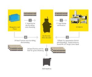
The closed-loop quality control (QC) system harnesses the power of the firm’s NEXIV VMZ-K3040 confocal (CF) 2D and 3D video measuring system, and couples it with robotic overhead transfer of the electronic devices to be tested. It eliminates the previous laborious need for an operator to handle a sample IC to a microscope, measure the critical parameters and then manually key in offsets to the die bonder and wire bonder’s control system.
The fast, reliable, fully automated Quality 4.0 process, which dovetails with the growing demand for Industry 4.0-compatible metrology, is applicable throughout the die bonding and wire bonding sector. It is becoming an important inspection technique following its pilot implementation at several world-renowned electronics manufacturing companies.
Noteworthy is that Nikon’s high definition optical equipment is able to cope with the increasing density of circuitry on semiconductor chips (dies), their ever smaller size and closer spacing, and the increasing number of bonded wires between each chip and the lead frame that surrounds it.
Example application at a printer head manufacturer
The Nikon equipment and software used in QC of die bond and wire bond in the lead frame’s IC mounting process is standard, but there is a bespoke element to each installation. The supplier provides up-front consultancy to determine how best to configure the system to inspect the various parameters, and to determine in each case whether the NEXIV machine’s 2D or 3D optics will produce the best result.
This holistic approach is well exemplified by the recent installation of a Nikon video measuring system at a well-known printer manufacturer, which required an improved method for controlling the quality of the IC that is responsible for extremely accurate control of the ink colours flowing from every printer head.
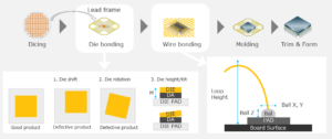
Numerous measurements have to be made to ensure each parameter on the IC is in tolerance and that it will work efficiently when mounted on the printer head. The features that need to be checked are die position in X and Y, die tilt, epoxy to die surface distance, wire bond ball diameter, ball height, ball position on the bond pad, bond thickness, and wire loop height and epoxy width from die edge.
Nikon engineers consulted with the customer, and all parties agreed that a K-series 2D / 3D CF video measuring machine was needed (which incidentally is used worldwide by major die bonding and wire bonding machine manufacturers), rather than a 2D-only system.
The decision to install this powerful CF inspection facility was down to five of the seven parameters being more precisely and quickly measured in 3D, namely the ball height and width, wire loop height, die tilt and epoxy height. Only ball placement and epoxy width are more expediently checked using the faster 2D process, which is just as accurate as 3D.
In this application, a Nikon Type-S 7.5x objective is used on the NEXIV VMZ-K3040, which has an inspection envelope of 300 x 400 x 150 mm. The lens has a 5 mm working distance and a 1.6 x 1.2 mm field of view (FOV) in confocal operation, with 0.25-micron height measurement repeatability, which is the 2-sigma value. FOV for brightfield 2D observation is 0.11 x 0.08 mm.
Wire bodning measurement (confocal)
Wire bonding measurement (brightfield)
Comparative studies showed that total inspection time using the CF system was nearly three times faster at 2 minutes 8 seconds compared with the 6 minutes it takes to measure the same features on a 2D-only machine. It is partly because Nikon’s CF design features the use of a Nipkow disc, raising inspection throughput compared with other confocal solutions on the market that use pinholes.
All elements of the system are compatible with SECS/GEM, the semiconductor industry’s standard interface protocol for automated fabrication. It orchestrates starting and stopping of the equipment, collection of metrology data, adjustment of variables, and distribution of recipes between 2D and 3D optics for optimally measuring the different features.
The process was integrated into the customer’s manufacturing execution system for automatically feeding back results to the die bonders and wire bonders to optimise their operation. The high throughput speed allows the first IC in a 25-position magazine per lot to be fully measured to a high level of accuracy. Offsets for any parameters found to be near to the tolerance limit are fed back to the die bonder and wire bonder so that all of the subsequent substrate mounting process are likely to be perfect. This is verified by sending all circuits to automatic optical inspection stations for gross checking.
A similarly successful automated QC process has been adopted by a manufacturer of SSD (solid state drive) chips, within which the critical parameters must be more stringently maintained due to the requirement to stack the ICs to form multi-layer memory cells.
Learn more about product: NEXIV VMZ-K Series


