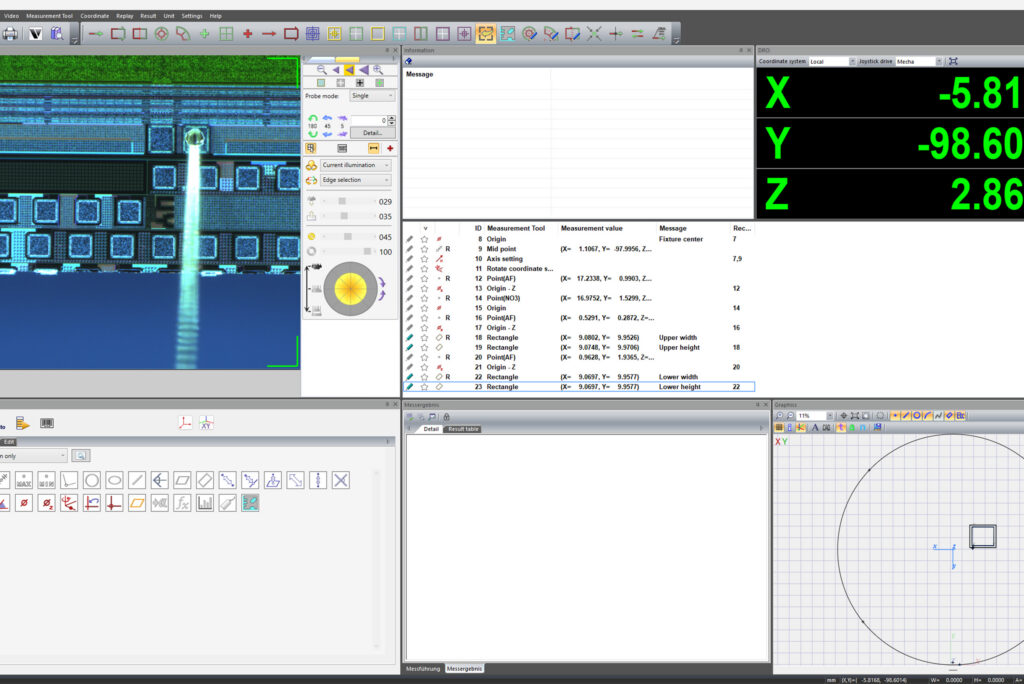
Thank you for joining our webinar on 29th February to learn how Nikon’s NEXIV VMZ-NWL200 video measuring system brings automation and precision to critical “micron-scale” measurements in semiconductor production, reducing costs and transforming process control capabilities.
Semiconductor production line measurements have never been more critical — or challenging. Yet traditional tools still leave key steps painfully manual, inefficient, and imprecise in some of the most important areas of semiconductor production.
And this is not an insignificant issue – as semiconductor wafers progress through production, their value increases, so catching issues before adding further layers saves money. Even tiny deviations can negatively impact device performance and reliability down the line, so accurate, efficient critical dimension (CD) measurement provides essential feedback.
However, the limitations of traditional tools mean measuring patterns over 1 μm becomes complex and qualitative manual work comparing images, making consistency and precision difficult.
Attendees will learn how this breakthrough technology can transform their process control capabilities and reduce the costs of manual measurement.
If you weren’t able to attend our webinar, here is the recording.


